Read Sharp LC-46X8E Service Manual online
LC-46X8E/S/RU
5 – 29
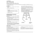
1.10. IC9602 (VHiMP2367DN-1Y)
1.10.1 Block Diagram
1.10.2 Pin Connections and short description
Pin No.
Pin Name
I/O
Pin Function
1
BS
I
High-Side Gate Drive Boost Input. BS supplies the drive for the high-side N-Channel MOSFET switch.
Connect a 0.01
Connect a 0.01
µF or greater capacitor from SW to BS to power the high side switch.
2
IN
I
Power Input. IN supplies the power to the IC, as well as the step-down converter switches.
Drive IN with a 4.75V to 28V power source. Bypass IN to GND with a suitably large capacitor to eliminate
noise on the input to the IC.
Drive IN with a 4.75V to 28V power source. Bypass IN to GND with a suitably large capacitor to eliminate
noise on the input to the IC.
3
SW
O
Power switching output. SW is the switching node that supplies power to the output. Connect the output LC
filter from SW to the output load. Note that a capacitor is required from SW to BS to power the high-side
switch.
filter from SW to the output load. Note that a capacitor is required from SW to BS to power the high-side
switch.
4
GND
—
Ground.
5
FB
I
Feedback Input. FB senses the output voltage to regulate that voltage. Drive FB with a resistive voltage
divider from the output voltage. The feedback reference voltage is 0.8V.
divider from the output voltage. The feedback reference voltage is 0.8V.
6
COMP
I
Compensation Node. COMP is used to compensate the regulation control loop. Connect a series RC net-
work from COMP to GND to compensate the regulation control loop. In same cases, an additional capaci-
tor from COMP to GND is required.
work from COMP to GND to compensate the regulation control loop. In same cases, an additional capaci-
tor from COMP to GND is required.
7
EN
I
Enable Input. EN is a digital input that turns the regulator on or off. Drive EN high to turn on the regulator,
drive it low to turn it off.
drive it low to turn it off.
8
SS
I
Soft-start Control Input. SS controls the soft-start period. Connect a capacitor from SS to GND to set the
soft-start period.
soft-start period.

