Read Sharp LC-M3700 (serv.man9) Service Manual online
34
LC-M3700
LC-M3710
LC-M3710
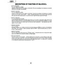
DESCRIPTION OF FUNCTION OF MAJOR ICs
•
IC4701 (IXA332WJ)
This IC is a QS driver for EVEN.
It QS (Quick Shoot)-drives the input signal sent from the DVI receiver according to the temperature parameter
setting from the monitor microcomputer.
This IC is a QS driver for EVEN.
It QS (Quick Shoot)-drives the input signal sent from the DVI receiver according to the temperature parameter
setting from the monitor microcomputer.
•
EIC4901 (IXA332WJ)
This IC is a QS driver for ODD.
It QS (Quick Shoot)-drives the input signal sent from the DVI receiver according to the temperature parameter
setting from the monitor microcomputer. In addition, after QS-driving the H and V synchronization signal and
DE signal sent from the DVI receiver, it outputs the H and V synchronization signal and DE signal.
•
EIC4501 (IXA457WJ)
This IC is a liquid crystal controller.
It allocate the video data of the 24-bit RGB signal, H and V synchronization signal and DE signal sent from the
QS driver (ODD and EVEN) to the left-side ODD and EVEN and the right-side ODD and EVEN of the liquid
crystal panel and outputs the control signal for driving the liquid crystal panel. It also generates the control
signal for dimmer control.
•
EIC4303 (IXA345WJ)
This IC is a CPLD.
Because the QS driver and liquid crystal controller are general-purpose FPGAs, it is used to make setting for
each FPGA. After resetting, it reads the program data from IC4301 (flash) and makes setting for each IC
through serial transmission.
This IC is a CPLD.
Because the QS driver and liquid crystal controller are general-purpose FPGAs, it is used to make setting for
each FPGA. After resetting, it reads the program data from IC4301 (flash) and makes setting for each IC
through serial transmission.
•
EIC4105 (IXA350WJ)
This IC is a gray scale reference power for TFT liquid crystal. It incorporates ten circuits of gray scale output
buffer amp, a CMOS buffer amp and a reference voltage supply.
This IC is a gray scale reference power for TFT liquid crystal. It incorporates ten circuits of gray scale output
buffer amp, a CMOS buffer amp and a reference voltage supply.
•
EIC2004 (IXA3491CE)
This IC is a monitor microcomputer. It performs OSD control of the monitor section, detection of the panel
temperature through the thermistor, setting of the temperature parameter for the OS driver, setting of the timing
for the liquid crystal controller, setting of the dimmer control data, power control of the monitor section, monitoring
of each power line, remote control decoding and OPC control.
35
LC-M3700
LC-M3710
LC-M3710
35-1
35-2
Ë
VHiTFP501++-1Q (ASSY:IC1104)
Panel Bus HDCP DIGITAL RECEIVER
»
Block Diagram
»
Pin Function
Pin No
.
P
in Name
I/O
Pin Function
79
AGND
—
Analog ground—Ground reference and current return for analog circuitry.
79
AGND
—
Analog ground—Ground reference and current return for analog circuitry.
82,85,88,91
AVDD
—
Analog VDD—Power supply for analog circuitry. Nominally 3.3V.
67
CAP
O
Bypass capacitorÅ\4.7 _F tantalum and 0.01 _F ceramic capacitors connected to ground.
41,40
CTL[2:1]
O
General purpose control signals—Used for user defined control. In normal mode
CTL1 is not powered down via PDO.
94
DDC_SA
1
Display data channel_serial address—I2C Slave address bit A0 for display data
channel (DDC). Refer to I2C Interface section for more details.
92
DDC_SCL
I/O
Display data channel_serial clock—I2C Clock for the DDC. External pullup
resistors = 10 k_ and 3.3V to lerant.
93
DDC_SDA
I/O
Display data channel_serial data—I2C Data for the DDC. External pullup
resistors = 10 k_ and 3.3V to lerant.
46
DE
O
Output data enable—Used to indicate time of active video display versus
nonactive display or blanking interval. During blanking, only HSYNC, VSYNC
and CTL1_2 are transmitted. During times of active display, or nonblanking,
only pixel data, QE[23:0] and QO[23:0], is transmitted.
High: active display interval
Low: blanking interval
1
DFO
I
Output clock data format—Controls the output clock (ODCK) format for either
TFT or DSTN panel support. For TFT support ODCK clock runs continuously.
For DSTN support ODCK only clocks when DE is high; otherwise, ODCK is held
low when DE is low.
High: DSTN support/ODCK held low when DE = low.
Low: TFT support/ODCK runs continuously.
5, 39, 68
DGND
—
Digital ground—Ground reference and current return for digital core.
6, 38
DVDD
Digital VDD—Power supply for digital core. Nominally 3.3V.
48
HSYNC
O
H
orizontal sync output
100
OCK_INV
I
ODCK Polarity _ Selects ODCK edge on which pixel data (QE[23:0] and QO
[23:0]) and control signals(HSYNC, VSYNC, DE, CTL1_2 ) are latched.
Normal mode:
High: latches output data on rising ODCK edge.
Low: latches output data on falling ODCK edge.
44
ODCK
O
Output data clock—Pixel clock. All pixel outputs QE[23:0] and QO[23:0]
(if in 2-pixel/clock mode) along with DE, HSYNC, VSYNC and CTL[2:1] are
synchronized to this clock.
19, 28,45, 58,76
OGND
—
Output driver ground—Ground reference and current return for digital output drivers.
18, 29,43, 57,78
OVDD
—
O
utput driver VDD—Power supply for output drivers. Nominally 3.3V.
2
P
D
I
Power down—An active low signal that controls the TFP501 power-down state.
During power down all output buffers are switched to a high-impedance state
and brought low through a weak pulldown. All analog circuits are powered down
and all inputs are disabled, except for PD.
If PD is left unconnected, an internal pullup defaults the TFP501 to normal operation.
High: normal operation
Low: power down
9
PDO
I
O
utput drive power down—An active low signal that controls the power-down
state of the output drivers.
During output drive power down, the output drivers (except SCDT and CTL1) are
driven to a high-impedance state. A weak pulldown slowly pulls these outputs to
a low level. When PDO is left unconnected an internal pullup defaults the
TFP501 to normal operation.
High: normal operation/output drivers on.
Low: output drive power down.
98
PGND
—
PLL ground _ Ground reference and current return for internal PLL.
4
PIXS
I
Pixel select—Selects between one or two pixel per clock output modes. During
2-pixel/clock mode, both even pixels, QE[23:0], and odd pixels, QO[23:0], are
output in tandem on a given clock cycle. During 1 pixel/clock, even and odd
pixels are output sequentially, one at a time, with the even pixel first, on the
even pixel bus, QE[23:0]. (The first pixel per line is pixel-0, the even pixel. The
second pixel per line is pixel-1, the odd pixel.)
High: 2 pixel/clock
Low: 1 pixel/clock
95
PROM_SCL
I/O
EEPROM_serial clock—I2C clock for EEPROM interface data. External pullup
resistors = 10 k_ and 3.3V to lerant.
96
PROM_SDA
I/O
EEPROM_serial data—I2C data for EEPROM interface data. External pullup
resistors = 10 k_ and 3.3V to lerant.
97, 99
PVDD (1, 2)
PLL VDD—Power supply for internal PLL. Nominally 3.3V.
36
LC-M3700
LC-M3710
LC-M3710
36-1
36-2
10_17
QE[0:7]
O
Even blue pixel output
—
Output for even and odd blue pixels when in 1-pixel/
clock mode. Output for even only blue pixel when in 2-pixel/clock mode. Output
data is synchronized to the output data clock, ODCK.
LSB: QE0/pin 10
MSB: QE7/pin 17
20_27
QE[8:15]
O
Even green pixel output
—
Output for even and odd green pixels when in 1-pixel/
clock mode. Output for even only green pixel when in 2-pixel/clock mode.
Output data is synchronized to the output data clock, ODCK.
LSB: QE8/pin 20
MSB: QE15/pin 27
30_37
QE[16:23]
O
Even red pixel output
—
Output for even and odd red pixels when in 1-pixel/clock
mode. Output for even only red pixel when in 2-pixel/clock mode. Output data is
synchronized to the output data clock, ODCK.
LSB: QE16/pin 30
MSB: QE23/pin 37
49_56
QO[0:7]
O
Odd blue pixel output
—
Output for odd only blue pixel when in 2-pixel/clock
mode. Not used, and held low, when in 1-pixel/clock mode. Output data is
synchronized to the output data clock, ODCK.
LSB: QO0/pin 49
MSB: QO7/pin 56
59_66
QO[8:15]
O
Odd green pixel output
—
Output for odd only green pixel when in 2-pixel/clock
mode. Not used, and held low, when in 1-pixel/clock mode. Output data is
synchronized to the output data clock, ODCK.
LSB: QO8/pin 59
MSB: QO15/pin 66
69_75,77
QO[16:23]
O
Odd red pixel output
—
Output for odd only red pixel when in 2-pixel/clock mode.
Not used, and held low, when in 1-pixel/clock mode. Output data is
synchronized to the output data clock, ODCK.
LSB: QO16/pin 69
MSB: QO23/pin 77
42
RSVD
O
Reserved
—
Must be tied high for normal operation.
80
Rx2+
I
Channel-2 positive receiver input Positive side of channel-2 T.M.D.S. low
voltage signal differential input pair.
Channel-2 receives red pixel data in active display and CTL2 control signal
during blanking.
81
Rx2_
I
Channel-2 negative receiver input
—
Negative side of channel-2 T.M.D.S. low
voltage signal differential input pair.
83
Rx1+
I
Channel-1 positive receiver input
—
Positive side of channel-1 T.M.D.S. low
voltage signal differential input pair. Channel_1 receives green pixel data in
active display and CTL1 control signal during blanking.
84
Rx1_
I
Channel-1 negative receiver input
—
Negative side of channel-1 T.M.D.S. low
voltage signal differential input pair.
86
Rx0+
I
Channel-0 positive receiver input
—
Positive side of channel-0 T.M.D.S. low
voltage signal differential input pair. Channel-0 receives blue pixel data in active
display and HSYNC, VSYNC control signals during blanking.
87
Rx0_
I
Channel-0 negative receiver input
—
Negative side of channel-0 T.M.D.S. low
voltage signal differential input pair.
89
Rx0+
I
Clock positive receiver input
—
Positive side of reference clock T.M.D.S. low
voltage signal differential input pair.
90
RxC_
I
Clock negative receiver input
—
Negative side of reference clock T.M.D.S. low
voltage signal differential input pair.
8
SCDT
O
Sync detect _ Output to signal when the link is active or inactive. The link is
considered to be active when DE is actively switching. The TFP501 monitors the
state DE to determine link activity. SCDT can be tied externally to PDO to
power down the output drivers when the link is inactive.
High: active link
Low: inactive link
3
S
T
I
Output drive strength select
—
Selects output drive strength for high or low
current drive. (see dc specifications for IOH and IOL vs ST state.)
High: high drive strength
Low: low drive strength
7
STAG
I
Staggered pixel select _ An active low signal used in 2 pixel/clock pixel mode
(PIXS = high). Time staggers the even and odd pixel outputs to reduce ground
bounce. Normal operation outputs the odd and even pixels simultaneously.
High: normal simultaneous even/odd pixel output.
Low: time staggered even/odd pixel output.
47
VSYNC
O
Vertical sync output
Pin No
.
Pin Name
I/O
Pin Function
Ë
VHiCXA2171Q-1Q (ASSY:IC8801)
Video/Sync Selector
»
Block Diagram
37
LC-M3700
LC-M3710
LC-M3710
37-1
37-2
»
Pin Function
Pin No
.
Pin Name
I/O
Pin Function
1
IN3_1
I
IN3 system signal input terminals.
2
IN3_2
I
Please input through a capacitor.
3
IN3_3
I
Bias of the terminal voltage is carried out to 2.9V.
An input Y level should give me 0.7Vp-p and a composit input level as 0.7Vp-p
with a color bar 100%.
In Sync on Y and Sync on Green, please input a Sync level by 0.3 Vp-p.
IN3_1 : Cr/Cb/R signal input
IN3_2 : Cb/Pb/B signal input
IN3_3 : Y/YHD/G signal input
4
IN3_H
I
IN3_H : They are an self-support H synchronization or the input terminal of CS.
5
IN3_V
I
IN3_V : It is the input terminal of an self-support V synchronized signal.
Please input through the capacitor for a clamp. A bottom level is clamped by 1V.
Corresponds to positive/negative two-poles nature.
Please input an input on the level shown below.
0.4Vp-p < IN3_H < 4Vp-p
0.4Vp-p < IN3_V <4Vp-p
6
GND3
—
GND of a synchronized signal system.
7
IN4_1
I
IN4 system signal input terminals.
8
IN4_2
I
Please input through a capacitor.
9
IN4_3
I
Bias of the terminal voltage is carried out to 2.9V.
An input Y level should give me 0.7Vp-p and a composit input level as 0.7Vp-p
with a color bar 100%.
In Sync on Y and Sync on Green, please input a Sync level by 0.3 Vp-p.
IN4_1 : Cr/Cb/R signal input
IN4_2 : Cb/Pb/B signal input
IN4_3 : Y/YHD/G signal input
10
IN4_H
I
IN4_H : They are an self-support H synchronization or the input terminal of CS.
11
IN4_V
I
IN4_V : It is the input terminal of an self-support V synchronized signal.
Please input through the capacitor for a clamp. A bottom level is clamped by 1V.
Corresponds to positive/negative two-poles nature.
Please input an input on the level shown below.
0.4Vp-p < IN4_H < 4Vp-p
0.4Vp-p < IN4_V < 4Vp-p
12
VCC3
—
Power supply terminal of a synchronized signal system.
13
H_PH
Capacitor connection terminal for carrying out the peak hold of the Hsync.
14
V_PH
Capacitor connection terminal for carrying out the peak hold of the Vsync.
15
YG_OUT
O
Composite Video signal output terminal for synchronous separation.
About 6dB of signals chosen by I2C bus "HYSW" is amplified, and they are
outputted.
16
YG_IN
I
Composite Video signal input terminal for synchronous separation.
Usually, the signal outputted by 15 pins is inputted through a clamp capacitor.
Sync Tip is clamped by 2.3V. Please input a Sync level by 0.5 - 0.6 Vp-p.
17
CLP_SW
I
Input terminal of the pulse which switches clamp circuit operation of Y signal system.
18
IREF
Reference current setting terminal in IC (synchronized signal processing system).
Please connect resistance 10kohm of less than 1% of errors to opposite GND
(metal leather film resistance etc.). Terminal voltage is about 1V.
19
NC
—
No connect
20
EXTCLK/XTAL
Reference clock change terminal for synchronous counters.
When using Inside VCO, it is set as I2C bus "CLK_SEL=0" and a 4MHz X'tal
oscillation element or a ceramic oscillation element is connected. When you
input the 4MHz clock of external, please set it as I2C bus "CLK_SEL=1."
21
NC
—
No connect
22
SELH_OUT
O
HV output terminal of selectors IN1-IN4.
VOH < 3.5V
23
SELV_OUT
O
VOL < 0.5V
24
GND2
—
GND terminal of a picture signal system.
25
SELCR_OUT
O
Output terminal of selectors IN1-IN4. The signal by which YCbCr conversion
was carried out is outputted.
An output level is outputted by 6dB of an input level, when it is set as I2C bus
"GAIN_SEL=0."
26
SELCB_OUT
O
27
SELY_OUT
O
28
VCC2
—
Power supply terminal of a picture signal system.
29
CLP_CR
It is a constant terminal at the time of a diode clamp.
The minimum potential of a signal is clamped to 1.4V.
30
SCL
I
SCL (Serial Clock) input terminal of I2C bus reference.
31
SDA
I
SDA (Serial Data) input terminal of I2C bus reference.
32
ADDRESS
slave address setting terminal of I2C bus.
8Eh : More than 4V
8Ch : Open
84h : Less than 1.5V
33
IN1_1
I
IN1 system signal input terminals.
34
IN1_2
I
Please input through a capacitor.
35
IN1_3
I
Bias of the terminal voltage is carried out to 2.9V.
An input Y level should give me 0.7Vp-p and a composit input level as 0.7Vp-p
with a color bar 100%.
In Sync on Y and Sync on Green, please input a Sync level by 0.3 Vp-p.
IN1_1 : Cr/Cb/R signal input
IN1_2 : Cb/Pb/B signal input
IN1_3 : Y/YHD/G signal input
36
IN1_H/L1
I
IN1_H : They are an self-support H synchronization or the input terminal of CS.
37
IN1_V/L2
I
IN1_V : It is the input terminal of an self-support V synchronized signal.
Please input through the capacitor for a clamp. A bottom level is clamped by 1V.
Corresponds to positive/negative two-poles nature.
Please input an input on the level shown below.
0.4Vp-p < IN1_H < 4Vp-p
0.4Vp-p < IN1_V < 4Vp-p
Moreover, when it is set as I2 C bus "SELSTB_1=1", it becomes the input
terminal of the control lines 1 and 2 of D3 terminal. DC level of an input is
returned to status register "DECL1_1" and "DECL 2_1" by Three values.
38
IN1_L3
I
Input terminal of the control line 3 of D3 terminal.
When it is set as I2C bus "SELSTB_1=1", Return DC level of an input to status
register "DECL3_1" with three values.
39
IN1_SW
I
Input terminal of the control line 3 of D3 terminal.
When it is set as I2C bus "SELSTB_1=1", Return DC level of an input to status
register "DECL3_1" with two values.
40
VCC1
—
Power supply terminal of an input selector.
41
IN2_1
I
IN2 system signal input terminals.
42
IN2_2
I
Please input through a capacitor.
43
IN2_3
I
Bias of the terminal voltage is carried out to 2.9V.
An input Y level should give me 0.7Vp-p and a composit input level as 0.7Vp-p
with a color bar 100%.
In Sync on Y and Sync on Green, please input a Sync level by 0.3 Vp-p.
IN2_1 : Cr/Cb/R signal input
IN2_2 : Cb/Pb/B signal input
IN2_3 : Y/YHD/G signal input
44
IN2_H/L1
I
IN2_H : They are an self-support H synchronization or the input terminal of CS.
45
IN2_V/L2
I
IN2_V : It is the input terminal of an self-support V synchronized signal.
Please input through the capacitor for a clamp. A bottom level is clamped by 1V.
Corresponds to positive/negative two-poles nature.
Please input an input on the level shown below.
0.4Vp-p < IN2_H < 4Vp-p
0.4Vp-p < IN2_V < 4Vp-p
Moreover, when it is set as I2 C bus "SELSTB_2=1", it becomes the input
terminal of the control lines 1 and 2 of D3 terminal. DC level of an input is
returned to status register "DECL1_2" and "DECL 2_2" by Three values.
46
IN2_L3
I
Input terminal of the control line 3 of D3 terminal.
When it is set as I2C bus "SELSTB_2=1", Return DC level of an input to status
register "DECL3_2" with three values.
47
IN2_SW
I
Input terminal of the switch line of D3 terminal.
When it is set as I2C bus "SELSTB_2=1", Return DC level of an input to status
register "DECSW_2" with two values.
48
GND1
—
GND of an input selector.
Pin No
.
Pin Name
I/O
Pin Function

