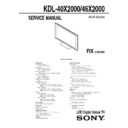
Read Sony KDL-40X2000 Service Manual online
HISTORY
Model Name :
SERVICE MANUAL
SERVICE MANUAL
Click on Page Number to display detail of changes.
KDL-40X2000
Date Part Number Description of Revisions
Version
1.0
9-927-536-01
2006.08
Original Manual.
2.0
9-927-536-02
2007.03
Correction of Section 5-3 to include missing parts
(P.86)
3.0
9-927-536-03
2008.03
Stand Assy part numbers for Black and Silver models
(P.85)
- 1 -
FIX
RM-ED006
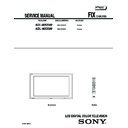
SERVICE MANUAL
FIX
CHASSIS
MODEL
COMMANDER
DEST
MODEL
COMMANDER
DEST
KDL-40X2000
RM-ED006
UK
RM-ED006
FLAT PANEL COLOR TV
KDL-40X2000
KDL-40X2000
RM-ED006
AEP
- 2 -
FIX
RM-ED006
TABLE OF CONTENTS
Section
Title
Page
Section
Title
Page
Caution ................................................................
3
Specifications ......................................................
4
Connectors ..........................................................
6
Self Diagnosis .....................................................
7
1. GENERAL
...................................................................
8
2. DISASSEMBLY
2-1.
Rear Cabinet Assy Removal ...............................
18
2-2.
Stand Base Assy Removal ..................................
19
2-3.
Loudspeaker Removal ........................................
19
2-4.
AE Board Removal .............................................
20
2-5.
B2 Board Removal ..............................................
20
2-6.
D1 Board Removal .............................................
21
2-7.
FXE Board Removal ..........................................
21
2-8.
G1 Board Removal .............................................
22
2-9.
H1 Board Removal .............................................
22
2-10. H2 Board Removal .............................................
23
2-11. H3 Board Removal .............................................
23
2-12. H4 Board Removal .............................................
24
2-13. TUE Board Removal ..........................................
24
2-14. Inverter Board Removal ......................................
25
2-15. LCD Panel Removal ...........................................
25
3. ADJUSTMENTS
3-1.
How to enter Service Mode ...............................
26
3-2.
White Balance Adjustment .................................
26
3-3.
Board Replacement .............................................
27
3-3-1. AE Board Replacement ...................................
27
3-3-2. B2 Board Replacement ....................................
27
3-3-3. TUE Board Replacement .................................
27
3-3-4. Fine Level Tuning - Analog RF input
(PAL, SECAM) / Y-Level ..............................
27
3-3-5. Fine Level Tuning - CVBS input
(PAL, SECAM) / Y-Level ..............................
27
3-4.
Trouble Shooting ...............................................
28
3-4-1. No Power ........................................................
28
3-4-2. Set Restarts ......................................................
28
3-4-3. Temperature Error ............................................
28
3-4-4. Over Voltage Protection (OVP) ......................
28
3-4-5. Power Error .....................................................
28
3-4-6. Audio Error .....................................................
28
3-4-7. Panel Error .......................................................
28
Audio Problem Flowchart ..............................
29
Video Problem Flowchart ..............................
29
4. DIAGRAMS
4-1.
Block Diagrams(1) .............................................
30
Block Diagrams(2) .............................................
31
Block Diagrams(3) .............................................
32
Block Diagrams(4) .............................................
33
Block Diagrams(5) .............................................
34
Block Diagrams(6) .............................................
35
Block Diagrams(7) .............................................
36
Block Diagrams(8) .............................................
37
4-2.
Circuit Board Location ........................................
37
4-3.
Schematic Diagrams and Printed Wiring
Boards .................................................................
37
AE Board Schematic Diagram ............................
38
AE Printed Wiring Board .................................
46
B2 Board Schematic Diagram .............................
49
B2 Printed Wiring Board ...................................
62
D1 Board Schematic Diagram ............................
64
D1 Printed Wiring Board ...................................
65
G1 Board Schematic Diagram ............................
67
G1 Printed Wiring Board ....................................
68
TUE Board Schematic Diagram ..........................
70
TUE Printed Wiring Board .................................
71
FXE Board Schematic Diagram ..........................
72
FXE Printed Wiring Board ...............................
77
H1 Board Schematic Diagram ............................
78
H1 Printed Wiring Board ..................................
79
H2 Schematic Diagram .......................................
78
H2 Printed Wiring Board ....................................
79
H3 Schematic Diagram .......................................
80
H3 Printed Wiring Board ....................................
79
H4 Schematic Diagram .......................................
80
H4 Printed Wiring Board ....................................
79
4-4.
Semiconductors ................................................... 81
5. EXPLODED VIEWS
5-1.
Chassis ................................................................
84
5-2.
Rear Cover and Stand .........................................
85
5-3.
Screen Assy ........................................................
86
6. ELECTRICAL PARTS LIST
.................................. 87
SAFETY-RELATED COMPONENT WARNING !!
COMPONENTS IDENTIFIED BY SHADING AND MARKED
ON
THE SCHEMATIC DIAGRAMS, EXPLODED VIEWS AND IN THE
PARTS LIST ARE CRITICAL FOR SAFE OPERATION. REPLACE
THESE COMPONENTS WITH SONY PARTS WHOSE PART
NUMBERS APPEAR AS SHOWN IN THIS MANUAL OR IN
SUPPLEMENTS PUBLISHED BY SONY.
PARTS LIST ARE CRITICAL FOR SAFE OPERATION. REPLACE
THESE COMPONENTS WITH SONY PARTS WHOSE PART
NUMBERS APPEAR AS SHOWN IN THIS MANUAL OR IN
SUPPLEMENTS PUBLISHED BY SONY.
WARNING !!
AN ISOLATION TRANSFORMER SHOULD BE USED DURING
ANY SERVICE WORK TO AVOID POSSIBLE SHOCK HAZARD
DUE TO LIVE CHASSIS, THE CHASSIS OF THIS RECEIVER IS
DIRECTLY CONNECTED TO THE POWER LINE.
ANY SERVICE WORK TO AVOID POSSIBLE SHOCK HAZARD
DUE TO LIVE CHASSIS, THE CHASSIS OF THIS RECEIVER IS
DIRECTLY CONNECTED TO THE POWER LINE.
- 3 -
FIX
RM-ED006
The circuit boards used in these models have been processed using
Lead Free Solder. The boards are identified by the LF logo located
close to the board designation e.g. F1, H1 etc [ see examples ]. The
servicing of these boards requires special precautions to be taken as
outlined below.
Lead Free Solder. The boards are identified by the LF logo located
close to the board designation e.g. F1, H1 etc [ see examples ]. The
servicing of these boards requires special precautions to be taken as
outlined below.
CAUTION
Lead Free Soldered Boards
example 1
example 2
It is strongly recommended to use Lead Free Solder material in order to guarantee optimal quality of new solder joints. Lead Free Solder is
available under the following part numbers :
available under the following part numbers :
Due to the higher melting point of Lead Free Solder the soldering iron tip temperature needs to be set to 370 degrees centigrade. This requires
soldering equipment capable of accurate temperature control coupled with a good heat recovery characteristics.
soldering equipment capable of accurate temperature control coupled with a good heat recovery characteristics.
For more information on the use of Lead Free Solder, please refer to http://www.sony-training.com
r
e
b
m
u
n
t
r
a
P
r
e
t
e
m
a
i
D
s
k
r
a
m
e
R
9
1
-
5
0
0
-
0
4
6
-
7
m
m
3
.
0
g
K
5
2
.
0
0
2
-
5
0
0
-
0
4
6
-
7
m
m
4
.
0
g
K
0
5
.
0
1
2
-
5
0
0
-
0
4
6
-
7
m
m
5
.
0
g
K
0
5
.
0
2
2
-
5
0
0
-
0
4
6
-
7
m
m
6
.
0
g
K
5
2
.
0
3
2
-
5
0
0
-
0
4
6
-
7
m
m
8
.
0
g
K
0
0
.
1
4
2
-
5
0
0
-
0
4
6
-
7
m
m
0
.
1
g
K
0
0
.
1
5
2
-
5
0
0
-
0
4
6
-
7
m
m
2
.
1
g
K
0
0
.
1
6
2
-
5
0
0
-
0
4
6
-
7
m
m
6
.
1
g
K
0
0
.
1


