Read Sony CDX-L400X (serv.man2) Service Manual online
1
AEP Model
UK Model
SERVICE MANUAL
Ver 1.1 2003. 08
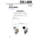
SUPPLEMENT-1
File this supplement with the service manual.
Subject : Change of CD Mechanism
(ECN-CSB03573)
CD mechanism changed into MG-393XA-121//Q and MG-393XC-121//Q from
MG-393X-121//Q in the middle of the production.
When performing service and inspection, check the suffix of the part number of
the servo board.
MG-393X-121//Q in the middle of the production.
When performing service and inspection, check the suffix of the part number of
the servo board.
CDX-L400X
9-873-438-81
Discrimination
SERVO BOARD Part No.
MG-393X-121//Q : 1-680-276-2
MG-393XA-121//Q, MG-393XC-121//Q : 1-683-660-1
MG-393X-121//Q : 1-680-276-2
MG-393XA-121//Q, MG-393XC-121//Q : 1-683-660-1
KSS-720A
KSS-271A
MG-393XA-121//Q
MG-393XC-121//Q
- SERVO BOARD (COMPONENT SIDE) -
2
TABLE OF CONTENTS
1. Schematic Diagram –CD Mechanism Section– ...................... 3
2. Printed Wiring Boards –CD Mechanism Section– .................. 4
3. Exploded Views ....................................................................... 7
3-1. CD Mechanism Section (1) ................................................. 7
3-2. CD Mechanism Section (2) ................................................. 8
3-3. CD Mechanism Section (3) ................................................. 9
4. Electrical Parts List ................................................................ 10
CDX-L400X
THIS NOTE IS COMMON FOR PRINTED WIRING
BOARDS AND SCHEMATIC DIAGRAMS.
(In addition to this, the necessary note is
printed in each block.)
BOARDS AND SCHEMATIC DIAGRAMS.
(In addition to this, the necessary note is
printed in each block.)
for schematic diagram:
• All capacitors are in µF unless otherwise noted. pF: µµF
• All capacitors are in µF unless otherwise noted. pF: µµF
50 WV or less are not indicated except for electrolytics
and tantalums.
and tantalums.
• All resistors are in
Ω
and
1
/
4
W or less unless otherwise
specified.
•
%
: indicates tolerance.
•
f
: internal component.
•
C
: panel designation.
•
A
: B+ Line.
• Power voltage is dc 14.4V and fed with regulated dc power
supply from ACC and BATT cords.
• Voltages are taken with a VOM (Input impedance 10 M
Ω
).
Voltage variations may be noted due to normal produc-
tion tolerances.
tion tolerances.
• Waveforms are taken with a oscilloscope.
Voltage variations may be noted due to normal produc-
tion tolerances.
tion tolerances.
• Circled numbers refer to waveforms.
• Signal path.
J
: CD
for printed wiring boards:
• X
: parts extracted from the component side.
• Y
: parts extracted from the conductor side.
•
a
: Through hole.
•
: Pattern from the side which enables seeing.
(The other layer’s patterns are not indicated.)
Note: The components identified by mark
0
or dotted line
with mark
0
are critical for safety.
Replace only with part number specified.
Caution:
Pattern face side: Parts on the pattern face side seen from the
(Side B)
Pattern face side: Parts on the pattern face side seen from the
(Side B)
pattern face are indicated.
Parts face side: Parts on the parts face side seen from the
(Side A)
(Side A)
parts face are indicated.
•
((
)) : Refer to page of Service manual.
• Waveforms
— Servo Board —
(MODE: CD PLAY)
1
2
3
IC1
ts
(PACK)
IC1
uj
(RFO)
1.5Vp-p
4
Approx. 100mVp-p
IC1
oa
(FEO)
0V
5
Approx. 100mVp-p
IC1
od
(TEO)
1.8Vp-p
16.9344MHz
IC1
wd
(XTAL)
5Vp-p
0V
3.3msec
3
3
CDX-L400X
• Refer to page 2 for Waveforms and Common Note on Schematic Diagram.
1. SCHEMATIC DIAGRAM — CD MECHANISM SECTION — • Refer to page 6 for IC Block Diagrams.
((Page 22))
Note:
• Voltage is dc with respect to
ground under no-signal conditions.
no mark : CD PLAY
no mark : CD PLAY
IC B/D
IC B/D
TP77
TP78
R29
R30
C43
TP79
TP80
TP80
TP81
TP82
TP82
TP83
TP84
TP84
CN2
CN3
SW3
M902
M901
SW2
SW1
TP2
TP3
M903
TP87
TP86
TP9
TP8
R3
R26
C4
TP10
C13
R5
C11
C10
C8
TP7
TP92
R6
TP15
TP14
TP17
TP20
TP16
TP16
TP19
TP21
TP18
BP4
BP3
R7
C17
TP11
TP12
C9
C14
TP89
C19
C20
C23
R9
R8
TP22
TP23
TP24
TP25
TP88
C26
TP31
BP1
BP2
TP33
TP32
R14
R15
TP30
R12
R10
TP91
TP90
TP29
TP28
TP26
TP27
R21
R22
R31
C44
TP34
TP35
TP36
TP46
TP37
TP38
TP39
TP40
TP41
TP42
TP43
TP44
TP45
CN1
R18
R19
R20
R17
TP66
TP62
TP47
TP63
TP48
TP49
TP64
TP50
TP51
TP52
TP68
TP53
TP69
TP54
TP70
TP55
TP71
TP56
TP72
TP57
TP73
TP58
TP74
TP59
TP75
TP60
TP76
TP61
IC1
X1
C1
C5
C3
TP93
TP94
TP94
TP95
TP96
TP96
TP97
TP98
TP98
TP85
C15
C16
C70
C24
C35
C38
C36
FB5
C25
C34
C71
C29
C27
C41
C22
C30
C18
Q1
IC2
CN1
C6
TP1
TP4
TP5
SW4
4
4
CDX-L400X
1
A
B
C
D
E
F
G
H
I
2
3
4
5
6
7
8
9
10
11
12
13
14
CN2
2. PRINTED WIRING BOARDS — CD MECHANISM SECTION — • Refer to page 2 for Common Note on Printed Wiring Boards.


