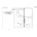
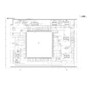
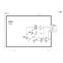
Read Sharp PZ-43MR2E (serv.man8) Service Manual online
20
PZ-43MR2E
PZ-50MR2E
PZ-50MR2E
Æ
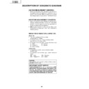
Description of Main ICs
»
»»
»»
IC1301 (CXA2069Q)
This IC is a 7-input, 3-output selector.
The video signals other than those for the PC, components and RGB input, which have been input from each input
connector and the tuner, and all the audio signals are sent to the IC1301 and then selected.
Output 1 is used internally and output 3 in the monitor output.
When the S video input is output to the monitor, Y and C signals are mixed in this IC.
The video signals sent to the IC1301 are then input to the YC separation circuits, IC405 (main) and IC402 (sub).
The audio signals are input to the PC I/F Unit via IC2501 (sound processor).
»
»»
»»
IC1401 (MM1519XQ)
This IC is a 4-input, 8-output video selector for component input.
The AV3 component input, AV1, RGB input, and Teletext RGB signals are input to the IC1401. The output signals
go to the main, sub, and component channels.
This IC is a 4-input, 8-output video selector for component input.
The AV3 component input, AV1, RGB input, and Teletext RGB signals are input to the IC1401. The output signals
go to the main, sub, and component channels.
»
»»
»»
IC1601 (SDA5550M).
This IC is a microprocessor for Teletext.
Video signals are input to the IC1601, which then decodes the Teletex data and outputs it as RGB data.
This IC is a microprocessor for Teletext.
Video signals are input to the IC1601, which then decodes the Teletex data and outputs it as RGB data.
»
»»
»»
IC2501 (IX3371CE)
This IC is used to decode audio signals.
It serves as both the S IF decoder and the selector for the input audio data.
This IC is used to decode audio signals.
It serves as both the S IF decoder and the selector for the input audio data.
»
»»
»»
IC801/IC802 (TB1274AF)
This IC synchronizes video and chroma signals for PAL/NTSC/SECAM colour televisions.
Its video circuit includes a high-performance image quality compensation circuit and its chroma circuit a PAL/
NTSC/SECAM automatic selection circuit. The PAL-M/N clock signals at 4.43 and 8.58 MHz are internally generated
for colour demodulation.
The PAL/SECAM demodulation circuit uses a base band signal processing system with built-in IH DL and is
therefore adjustment-free.
The IC801/IC802 has 4 lines for YC signal input, 2 lines for RGB signal input, and 2 lines for colour difference
signal input. It receives colour different signals for the main and sub channels from IC405 (main), IC402 (sub), and
IC1401 in the former stage, and provides 1 line for colour difference signal output.
»
»»
»»
IC803 (CXA2101Q)
This IC consists of a base band signal processing section for colour different input, an RGB signal processing
section, and a 4-line video switch (including HV synchronizing signal processing).
Input selection is performed by INPUT-SEL (I
This IC consists of a base band signal processing section for colour different input, an RGB signal processing
section, and a 4-line video switch (including HV synchronizing signal processing).
Input selection is performed by INPUT-SEL (I
2
C BUS). YCbCr, HD YPbPr, GBR and their respective HV synchronizing
signals are input to each line.
As the multi-scanning compliance range, a horizontal scanning frequency of 15~60 kHz can be input.
As the multi-scanning compliance range, a horizontal scanning frequency of 15~60 kHz can be input.
»
»»
»»
IC1901 (IX3566CE)
This IC is FPGA for the synchronizing system.
It creates sand castle pulses for IC803 and generates horizontal blanking signals.
This IC is FPGA for the synchronizing system.
It creates sand castle pulses for IC803 and generates horizontal blanking signals.
»
»»
»»
IC604 (TA1318AF)
This IC synchronizes TV component signals.
The IC804 incorporates the necessary functions for measuring the frequency of input signals and synchronous
replay into a single chip, and is applicable for horizontal synchronous replay (15.75, 31.5, 33.75, and 45 kHz) and
vertical synchronous replay (525I, 525P, 625I, 750P, 1125I, 1125P, PAL 100 Hz, and NTSC 120 Hz).
DESCRIPTION OF MAJOR IC FUNCTIONS
21
PZ-43MR2E
PZ-50MR2E
PZ-50MR2E
»
»»
»»
IC405/IC402 (CXD2064Q)
This IC is a comb filter in the applicable field for both the NTSC and PAL systems. It performs the Y/C separation
of the main and sub channel video signals that have been output from IC1801.
This IC is a comb filter in the applicable field for both the NTSC and PAL systems. It performs the Y/C separation
of the main and sub channel video signals that have been output from IC1801.
»
»»
»»
IC407/IC404 (ML6428C1)
This IC is a 6.7 MHz low-pass filter.
This IC is a 6.7 MHz low-pass filter.
»
»»
»»
IC810/IC804 (IX3473CE)
This IC is a 6.7 MHz low-pass filter incorporating a 6 dB amplifier.
This IC is a 6.7 MHz low-pass filter incorporating a 6 dB amplifier.
»
»»
»»
IC811 (IX3474CE)
This IC is a 30 MHz low-pass filter incorporating a 6 dB amplifier.
This IC is a 30 MHz low-pass filter incorporating a 6 dB amplifier.
»
»»
»»
IC1702 (FA3675CE)
This IC is designed to control the 6-channel PWM switching regulator.
With 5 step-up switching regulator lines incorporated, the IC converts +10V to +2.5V, +3.3V and +5.8V.
Also with a step-down switching regulator line incorporated, the IC converts +10V to +6.0V, -5.0V, +12V and +35V.
The lines are individually turned on and off.
Æ
Description of Functions of Main ICs on PC I/F Unit
»
»»
»»
IC4 (CXA3506R)
This IC is an A/D converter that incorporates a 3-channel, 8-bit, 120 MSPS amplifier and PLL. It is used for the
video signals input to the PC I/F unit on the main channel in the 1-screen and 2-screen modes, and also for the
video signals input from the front for the PC.
The video signals (analog RGB) from the CN6 are input to IN1 of IC4.
For the PC, the video signals (analog RGB) from CN8 are input to IN2 of IC4.
The input video signals are converted into digital signals and then sent to IC25.
»
»»
»»
IC310 (TLC5733A)
This IC is a 3-channel, 8-bit, 20 MSPS A/D converter.
It is used for the sub-channel of the video signals input to the PC I/F Unit in the 2-screen mode.
The video signals (analog Y, Cb, Cr) from CN6 are input to IC310.
The video signals input to this IC are converted into digital signals and then sent to IC25.
»
»»
»»
IC25 (IX3434CE)
This IC performs the I/P conversion and scaling to match the digitalized video with the output resolution, and also
the data conversion.
It has two input lines, V0 and V1. The V0 line is used to process the RGB, composite, and skirt signals input to the
480i and 580i components for the sub-channel in the 2-screen mode. The V1 line is used to process all the signals
as well as V1 for the main channel in the 1-screen and 2-screen modes.
The IC25 detects what resolution is input from the input synchronizing signal; creates H synchronization in
accordance with the frequency division ratio; creates the clamp signal in accordance with the input synchronizing
signal; and performs the data matrix conversion.
The video signals input to this IC is sent to IC413.
»
»»
»»
IC413 (SiI168)
This IC is a panel link transmitter.
It converts the 8-bit RGB video data output from IC25 into the differential TMDS signals and then digitally transmits
the converted signals to the monitor.
The TMDS signals are transmitted at the frequency 10 times higher than the clock frequency.
This IC is a panel link transmitter.
It converts the 8-bit RGB video data output from IC25 into the differential TMDS signals and then digitally transmits
the converted signals to the monitor.
The TMDS signals are transmitted at the frequency 10 times higher than the clock frequency.
»
»»
»»
IC1 (IX3270CE)
This IC is a 1-chip RISC microprocessor.
It performs communication with the monitor and operates the system.
The IC1 also controls each IC in the AVC system and partially manages the power source.
This IC is a 1-chip RISC microprocessor.
It performs communication with the monitor and operates the system.
The IC1 also controls each IC in the AVC system and partially manages the power source.
»
»»
»»
IC405 (uPD4721)
This IC is an RS-232 line driver receiver conforming to the EIA/TIA-232-E standard.
The IC405, when connected to a PC, allows for externally controlling the system.
It is also applicable for upgrading IC1.
This IC is an RS-232 line driver receiver conforming to the EIA/TIA-232-E standard.
The IC405, when connected to a PC, allows for externally controlling the system.
It is also applicable for upgrading IC1.
22
PZ-43MR2E
PZ-50MR2E
PZ-50MR2E
»
The information shown in the list is basic information and may not correspond exactly to that shown in the schematic diagrams.
Ë
VHiCXA2069Q-1 (ASSY: IC1301)
»
S2-Compatible, 7-Input/3-Ouput AV Switch
»
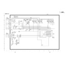
Block Diagram
23
PZ-43MR2E
PZ-50MR2E
PZ-50MR2E
63
1
8
15
22
30
60
3
10
17
24
49
5
12
19
26
51
62, 2
9, 16
23, 29
59, 64
4, 11
18, 25
31, 61
53
41
44
1
8
15
22
30
60
3
10
17
24
49
5
12
19
26
51
62, 2
9, 16
23, 29
59, 64
4, 11
18, 25
31, 61
53
41
44
56
39
58
47
37
52
43
38
54
45
40
6
13
20
27
7
14
21
28
32
39
58
47
37
52
43
38
54
45
40
6
13
20
27
7
14
21
28
32
33
34
36
34
36
55
46
48
46
48
50
»
Pin Function
Pin No.
Pin Name
I/O
Pin Function
TV
V1
V2
V3
V4
V5
V6
Y1
Y2
Y3
Y4
YIN1
C1
C2
C3
C4
CIN1
LTV, LV1
LV2, LV3
LV4, LV5
LV6, RTV
RV1, RV2
RV3, RV4
RV5, RV6
VOUT1
VOUT3
V/YOUT2
V1
V2
V3
V4
V5
V6
Y1
Y2
Y3
Y4
YIN1
C1
C2
C3
C4
CIN1
LTV, LV1
LV2, LV3
LV4, LV5
LV6, RTV
RV1, RV2
RV3, RV4
RV5, RV6
VOUT1
VOUT3
V/YOUT2
YOUT1
YOUT3
COUT1
COUT2
COUT3
LOUT1
LOUT2
LOUT3
ROUT1
ROUT2
ROUT3
S2-1
S2-2
S2-3
S2-4
S-1
S-2
S-3
S-4
ADR
YOUT3
COUT1
COUT2
COUT3
LOUT1
LOUT2
LOUT3
ROUT1
ROUT2
ROUT3
S2-1
S2-2
S2-3
S2-4
S-1
S-2
S-3
S-4
ADR
SCL
SDA
DC OUT
SDA
DC OUT
TRAP1
TRAP2
MUTE
TRAP2
MUTE
BIAS
I
I
I
I
I
I
I
I
I
I
I
I
I
I
I
I
I
I
I
I
I
I
I
I
I
I
I
I
I
I
I
I
I
I
I
I
I
I
I
I
I
I
I
I
I
I
I
O
O
O
O
O
O
O
O
O
O
O
O
O
O
O
O
O
O
O
O
O
O
O
O
O
O
I
I
I
I
I
I
I
I
I
I
I
I
I
I
I
I
I
I
I
I
O
I
I
I
I
I
I
Video signal input.
Composite video signal input
Composite video signal input
Y/C-separated signal input terminal for luminance signal input.
YIN1 to feed in the Y/C-separated signal of VOUT1 output.
YIN1 to feed in the Y/C-separated signal of VOUT1 output.
Y/C-separated signal input terminal for chrominance signal input.
CIN1 to feed in the Y/C-separated signal of VOUT1 output.
CIN1 to feed in the Y/C-separated signal of VOUT1 output.
Audio signal input terminal.
Video signal output terminal for composite video signal output.
Video signal output terminal for selection between composite video signal output and
luminance signal output by I2C Bus control.
Video signal output terminal for luminance signal output.
luminance signal output by I2C Bus control.
Video signal output terminal for luminance signal output.
Video signal output terminal for chrominance signal output.
Audio signal output terminal.
Used to detect C signal-superimposed, S2-compatible DC level. 4:3 video signal when
below 1.3V. 4:3 letterbox signal when between 1.3V and 2.5V. 16:9 image squeeze
signal when above 2.5V. To be pulled down to GDN at 100K
below 1.3V. 4:3 letterbox signal when between 1.3V and 2.5V. 16:9 image squeeze
signal when above 2.5V. To be pulled down to GDN at 100K
Ω
to produce 4:3 video
signal when open.
Used to switch between composite video and S signals. Detection results to be written
in status register. S signal when below 3.5V. Composite video signal when above 3.5V.
To be pulled up to 5V at 100K
Used to switch between composite video and S signals. Detection results to be written
in status register. S signal when below 3.5V. Composite video signal when above 3.5V.
To be pulled up to 5V at 100K
Ω
to produce composite video signal when open.
Used to select I2C Bus slave address. 90H when below 1.5V. 92H when above 2.5V.
90H also when the terminal is open.
I2C Bus signal input terminal.
I2C Bus signal input terminal.
Used to feed out S2-compatible DC level to be superimposed on COUT3 output. DC to
be superimposed by connecting to COUT3 output via a capacitor. Control to be made
by I2C Bus. S2-specified output impedance of 10 ±3K
Ω
to be realized by adding an
external resistance of 4.7K
Ω
.
Subcarrier trap circuit to be connected.
Audio signal output mute terminal. Mute off when below 1.3V. Mute on when above
2.5V. Mute off when the terminal is open.
Internal reference bias (Vcc/2) terminal. To be connected to GND with a capacitor in
between.
2.5V. Mute off when the terminal is open.
Internal reference bias (Vcc/2) terminal. To be connected to GND with a capacitor in
between.

