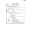
Read Sharp LC-30HV4E (serv.man10) Service Manual online
52
LC-30HV4E
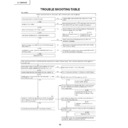
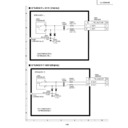
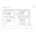
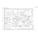
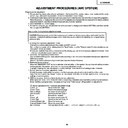
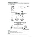
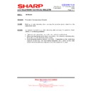
Power cannot be turned on. (The power LED on the front panel does not light up).
AVC System
Is the power cable connected properly?
Is fuse (F701) in order?
Is the BU+5V line (pin 1 of P1703) in order?
Are the wire harness and FFC connected properly?
Are DC/DC converter outputs and MOS-FET (Q1707 and
Q1708) in order?
Q1708) in order?
Replace IC1703.
Does the voltage of the OVP line (pin 8 of P1702) fluctuate
after power-on?
after power-on?
Plug the power cable connector and retry to turn on the
power.
power.
Replace the fuse and retry to turn on the power. If the fuse burns,
check VA701, D701 and IC701 and replace if necessary.
check VA701, D701 and IC701 and replace if necessary.
Check the BU+5V line for correct impedance. (Measure the
resistance between Pin 1 and GND).
resistance between Pin 1 and GND).
Check connections of the wire harness and FFC and
reconnect if necessary.
reconnect if necessary.
Check power supply internal devices (IC701, IC72, PC702,
Q702, D708 and D705).
Q702, D708 and D705).
Check DC/DC converter output lines and MOS-FET (Q1707
and Q1708) and replace if necessary.
and Q1708) and replace if necessary.
The power does not turn on even through the power button is pressed. (The red power LED on the front panel does not turn green or
is blinking red).
is blinking red).
Remove the cause of fault or
short-circuit.
short-circuit.
Check IC1702 and its
peripheral circuits.
peripheral circuits.
NO
YES
YES
YES
YES
YES
YES
YES
YES
YES
YES
YES
YES
YES
YES
YES
NO
NO
NO
NO
NO
NO
NO
NO
NO
NO
NO
NO
NO
NO
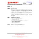
Is the system cable connected properly between the Display
and the AVC System (between DISPLAY OUTPUT(1)’s)?
and the AVC System (between DISPLAY OUTPUT(1)’s)?
Reconnect and retry to turn on the power.
Are the power switches of the Display and AVC System on?
Turn on the power switches of the Display and AVC System.
Are the UR+6V, UR+10V and UR+13V lines (pins 1, 2, 7 and
9 of P1702) in order?
9 of P1702) in order?
Are the D+1.8VCV line (pins 5 and 6 of P1701), D+3.3V line
(pin 8 of P1701), D+5V line (pin 1 of P1701) and A+5V line
(pin 3 of P1701) in order?
(pin 8 of P1701), D+5V line (pin 1 of P1701) and A+5V line
(pin 3 of P1701) in order?
Check the wire harness and FFC for proper connection.
Is PS_ON (pin 3 of P1702) pulled high (3.5V)?
Is D_POW (pins 32 and 34 of IC1703, pin 2 of IC1704 and
pin 2 of IC1705) pulled high?
pin 2 of IC1705) pulled high?
Is the impedance of the UR+6V, UR+10V and UR+13V lines
correct? (Measure the resistance between pins 1/2/7/9 of
P1072) and GND).
correct? (Measure the resistance between pins 1/2/7/9 of
P1072) and GND).
Check the PS_ON line.
Check the UR+6V, UR+10V and
UR+13V lines and devices on the
lines.
UR+13V lines and devices on the
lines.
Are MOS-FET (Q1707 and Q1708) and REG. IC (IC1704 and
IC1705) in order?
IC1705) in order?
Check the D_POW line (pin 6 of
IC1503).
IC1503).
Check each output line and replace MOS-FET (Q1707 and
Q1708) and REG. IC (IC1704 and IC1705).
Q1708) and REG. IC (IC1704 and IC1705).
Replace IC1703.
TROUBLE SHOOTING TABLE
53
LC-30HV4E
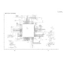
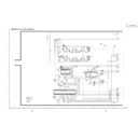
No sound (1)
No sound (2)
A
VC System
No sound (3)
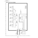
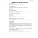
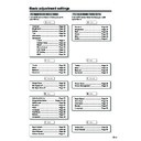
No sound is heard from the speaker in all modes.
Check audio circuits of the Display
.
Is the monitor audio output set to "V
ariable"? Or
Is the headphone connected?
Are the audio outputs of IC2501 (multi-sound
processor) in order?
Pins 36 and 37 of IC2501 (SC1 OUT
L/R).
Check IC2501 (multi-sound processor) and its
peripheral circuits.
Check lines and devices between pins 36/37 of
IC2501 and pins 1/3 of the
A
V
unit connector
(P2502). (Q2504-5, Q2509-10 and Q2513-4)
Set the monitor audio output to "Fixed".
Remove the headphone.
The speaker generates no sound when audio signals are inputted from an external device or a PC.
Check IC1301 (A
switch) and its peripherals.
Are the audio outputs of IC1301 (A
V switch) in
order?
Pins 52 and 54 of IC1301 (TV MAIN OUT
L/R)
Are the audio inputs of IC1301 (A
V switch) in
order?
Input 1: Between pins 2 and 4 of IC1301
Input 2: Between pins 9 and 1
1
of IC1301
Input 3: Between pins 16 and 18 of IC1301
Input 4: Between pins 23 and 25 of IC1301
PC input: Between pins 29 and 31 of IC1301
Are the audio input circuits of IC1301 (A
V switch)
in order?
Input 1: Between pins 6/2 and pins 2/4 of IC1301
Input 2: Between pins 6/2 and pins 9/1
1 of IC1301
Input 3:
Between pins 6/2 and pins 16/18 of IC1301
Front panel input: Between J2404 and pins 23/25
of IC1301
PC input: Between J2403 and pins 29/31 of IC1301
Are the audio inputs of IC2501 (multi-sound
processor) in order?
Pins 56 and 57 of IC2501 (SCI IN1 L/R)
YES
NO
YES
YES
YES
NO
NO
NO
No audio output <Input1>
No audio output <INPUT2/3>
Has the input mode been selected on the Input Select screen?
Are the audio outputs of IC2501 (multi-sound
processor) in order?
Pins 27 and 28 of IC2501 (DRCM L/R)
Check lines and devices between pins 27/28 of
IC2501 and pins 3/1 of INPUT1.
Also check the
audio mute circuits.
(IC2504, Q1
101-2)
Are the audio outputs of IC1301 (A
V switch) in
order?
Pins 43 and 45 of IC1301 (SC1
TV SUB OUT
L/R)
Check lines and devices between pins 43/45 of
IC1301 and pins 3/1 of INPUT2/3.
Also check
the audio mute circuits.
(IC1301, Q1
104-7 and Q1
109-12)
No monitor audio output or abnormal audio
The audio level is abnormal:
Is the monitor audio output set correctly?
"V
ariable" or "Fixed"
NO
YES
No sound at all:
Are the audio outputs of IC2501 (Multi-sound
processor) in order?
Pins 34 and 33 (SC2 OUT
L/R) of IC2501
Check lines and devices between pins 34/33 of
IC2501 and the monitor output (J1
101).
Also
check the audio mute circuit.
(Q2502-3, Q1
1
14-5 and Q1
106-7)
YES
Check peripherals of the SR unit DISPLA
Y
OUTPUT
2 pin (SC6000).
YES
YES
YES
YES
YES
Are audio signals applied to the
A
V
unit
connectors (pins 1 and 3 of P2502)?
YES
The speaker generates no sound when
TV signal is received.
Are the tuner audio inputs of IC2501 (multi-sound
processor) in order?
Pin 67 (sound IF1) of IC2501
Pin 69 (sound IF2) of IC2501
Is the audio signal applied to tuner output pin 21?
Check B.P
.F
. of SIF1 and SIF2.
(Q1
1
19-20 and Q1
121-2)
Check IC2501 (multi-sound processor) and its
peripheral circuits.
YES
YES
NO
NO
Check
TU1
101 (U/V tuner) and its peripherals.
54
LC-30HV4E
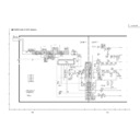
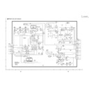
No image (1)
A
VC System
YES
NO
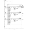
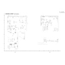
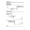
No video image on INPUT1
Has "INPUT1" been selected on the Input
Select screen?
Select INPUT1 CVBS on the Input Select
screen.
YES
NO
Is the video signal applied to pin 1 of IC1301
(A
V switch)?
Check lines and devices between pin 20 of
INPUT1 (SC1
101) and pin 1 of IC1301.
YES
NO
Select INPUT2 CVBS on the Input Select
screen.
YES
YES
(A)
(B)
YES
NO
Is the video signal applied to pin 8 of IC1301
(A
V switch)?
Check lines and devices between pin 20 of
INPUT2 (SC1
102 1/2) and pin 8 of IC1301.
NO video image on INPUT2
Has "INPUT2" been selected on the Input
Select screen?
<When video signal is received>
No image (2)
YES
NO
NO video image on INPUT3
Has "INPUT3" been selected on the Input
Select screen?
Select INPUT3 CVBS on the Input Select
screen.
YES
NO
Is the video signal applied to pin 1 of IC1301
(A
V switch)?
Check lines and devices between pin 20 of
INPUT3 (SC1
102 1/2) and pin 15 of IC1301.
YES
NO
Select INPUT4 CVBS on the Input Select
screen.
YES
YES
(C)
(D)
YES
NO
Is the video signal applied to pin 22 of
IC1301 (A
V switch)?
Check lines and devices between pin 3 of
INPUT4 (J2404) and pin 22 of IC1301.
NO video image on INPUT4
Has "INPUT4" been selected on the Input
Select screen?
<When video signal is received>
No image (3)
YES
NO
No
Y/C image on INPUT2
Has "INPUT2" been selected on the Input
Select screen?
Select INPUT2
Y/C on the Input Select
screen.
YES
NO
Is the
Y/C signal applied to pins 10 and 12
of IC1301 (A
V switch)?
Check lines and devices between pins20/15 of
INPUT1 (SC1
101) and pins 10/12 of IC1301.
YES
NO
Select INPUT3
Y/C on the Input Select
screen.
YES
YES
(E)
(F)
YES
NO
Is the
Y/C signal applied to pins 17 and 19
of IC1301 (A
V switch)?
Check lines and devices between pins20/15
of INPUT2 (SC1
102 1/2) and pins 17/19 of
IC1301.
No
Y/C image on INPUT3
Has "INPUT3" been selected on the Input
Select screen?
<When
Y/C signal is received>
No image (4)
YES
NO
No
Y/C image on INPUT4
Has "INPUT4" been selected on the Input
Select screen?
Select INPUT4
Y/C on the Input Select
screen.
YES
NO
Is the
Y/C signal applied to pins 24 and 262
of IC1301 (A
V switch)?
Check lines and devices between pins3/4 of
INPUT1 (J2401) and pins 24/26 of IC1301.
YES
(G)
<When
Y/C signal is received>
55
LC-30HV4E
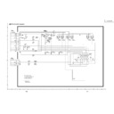
(A),(C),(E),(G)
(B),(D),(F)
<When video signal is received>
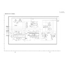
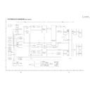
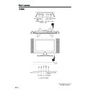
Are the main video signal and sub video signal sent from pin 56 and pin 44 of IC1301 respective
ly?
<When
Y/C signal is received>
Are the main
Y
signal, main C signal, sub
Y
signal and sub C signal sent from pin 56, pin 58, pin
44 and pin 47 of
IC1301 respectively?
Check IC1301 (A
V switch) and its peripheral
circuits.
<When video signal is received> Is the video signal applied to pin 7 of IC401 (main comb filter) and pin 7 of IC402 (sub comb f
ilter)?
<When
Y/C signal is received>
Are the main signal and sub signal applied to pins 44 and 43 of IC801 (main video chroma) and pin
s 5 and 7 of IC802
(sub video chroma) respectively?
Check lines and devices between IC1301
and IC401/IC402/IC801/IC802.
<Main system>
YES
YES
YES
YES
YES
YES
YES
YES
YES
YES
YES
YES
YES
NO
NO
NO
NO
NO
NO
NO
NO
NO
NO
NO
NO
NO
<When video signal is received>
Are the main
Y
signal and main C signal
applied to pin 1 (TP812) and pin 48 of
IC801 (main video chroma) respectively?
<When video signal is received>
Check lines and devices between IC4001
and IC801.
(IC403, Q415, etc.)
<When
Y/C signal is received>
Are the main
Y
signal and main C signal
applied to pin 44 and pin 43 of IC801 (main
video chroma) respectively?
<When
Y/C signal is received>
Check lines and devices between IC1301
and IC801.
(Q827, Q403, Q404, etc.)
Are the main
Y
, Cb and Cr signals sent
from pins 21, 22 and 23 of IC801
Check IC801 (main video chroma) and its
peripheral circuits.
Are the main
Y
, Cb and Cr signals applied to
pins 69, 68 and 67 of IC803 (RGB decoder)
Check lines and devices between IC801
and IC803. (IC814, Q814, Q815, etc.)
Are the main R, G and B signals sent from
pins 35, 37 and 39 of IC803 respectively?
Check IC803 (RGB decoder) and its
peripheral circuits.
Are the main R, G and B signals applied to
pins 3, 7 and 10 of FL810 (6.7/30 MHz
L.P
.F
.) respectively?
Are the main R, G and B signals sent from
pins 19, 15 and 12 of FL810 respectively?
Check lines and devices between IC803
and FL810.(Q801-3 etc.)
Is cutof
f frequency setting pin 17 of FL810
(6.7/30 MHz L.P
.F
.) pulled high?
Check FL810 (6.7/30 MHz L.P
.F
.) and its
peripheral circuits.
Check the PC I/F unit.
<Sub system>
<When video signal is received>
Are the sub
Y
signal and sub C signal
applied to pin 1 and pin 7 of IC802 (sub
video chroma) respectively?
<When video signal is received>
Check lines and devices between IC402
and IC802.
(IC404, Q416-8, etc.)
<When
Y/C signal is received>
Are the sub
Y
signal and sub C signal
applied to pin 5 and pin 7 of IC802 (sub
video chroma) respectively?
<When
Y/C signal is received>
Check lines and devices between IC1301
and IC802.
(IC828, Q409, Q410, etc.)
Are the sub
Y
, Cb and Cr signals sent from
pins 21, 22 and 23 of IC802 respectively?
Check IC802 (sub video chroma) and its
peripheral circuits.
Are the sub
Y
, Cb and Cr signals applied to
Q901-2, Q903-4 and Q905-6 (6.7 MHz
L.P
.F
.) respectively?
Check lines and devices between IC802
and Q901-2/Q903-4/Q 905-6 (6.7 MHz
L.P
.F
.).
Are the sub R, G and B signals sent from
Q901-2, Q903-4 and Q905-6 (6.7 MHz
L.P
.F
.) respectively?
Check peripherals of Q901-2, Q903-4 and
Q905-6 (6.7 MHz L.P
.F
.).

