Read Sharp LC-20B6E (serv.man10) Service Manual online
32
LC-20B6E
V
CCE
, V
CCI
,
V
SS
CNV
SS
X
IN
X
OUT
BYTE
P0
0
to P0
7
Signal name
Power supply
input
input
CNV
SS
Reset input
Clock input
Clock output
External data
bus width
select input
bus width
select input
I/O port P0
Supply 4.75V to 5.25V to the V
CCE
pin. Supply 3.15V to 3.45V to the
V
CCI
pin. Supply 0V to the V
SS
pin.
Function
This pin switches between processor modes. Connect it to the
V
V
SS
pin when operating in single-chip or memory expansion mode.
Connect it to the V
CCI
pin when in microprocessor mode.
A “L” on this input resets the microcomputer.
These pins are provided for the main clock generating circuit.Connect
a ceramic resonator or crystal between the X
a ceramic resonator or crystal between the X
IN
and the X
OUT
pins. To
use an externally derived clock, input it to the X
IN
pin and leave the
X
OUT
pin open.
This pin selects the width of an external data bus. A 16-bit width is
selected when this input is “L”; an 8-bit width is selected when this
input is “H”. This input must be fixed to either “H” or “L.” When
operating in single-chip mode,connect this pin to V
selected when this input is “L”; an 8-bit width is selected when this
input is “H”. This input must be fixed to either “H” or “L.” When
operating in single-chip mode,connect this pin to V
SS
.
This is an 8-bit CMOS I/O port. It has an input/output port direction
register that allows the user to set each pin for input or output
individually. When set for input in single-chip mode, the user can specify
in units of four bits via software whether or not they are tied to a pull-up
resistor. In memory expansion and microprocessor modes, the user
cannot specify that.
Pin name
Input
Input
Input
Output
Input
Input/output
I/O type
D
0
to D
7
P1
0
to P1
7
I/O port P1
0
7
These pins input and output data (D –D ).
This is an 8-bit I/O port equivalent to P0.
Input/output
Input/output
D
8
to D
15
P2
0
to P2
7
A
0
to A
7
I/O port P2
These pins input and output data
(D
8
–D
15
).
This is an 8-bit I/O port equivalent to P0.
These pins output 8 low-order address bits (A
0
–A
7
).
Input/output
Input/output
Output
RESET
81
50
82
49
83
48
84
47
85
46
86
45
87
44
88
43
89
42
90
41
91
40
92
39
93
38
94
37
95
36
96
35
97
34
98
33
99
32
100
7
6
5
4
3
2
1
0
2
1
0
P0
7
/D
P0
6
/D
P0
5
/D
P0
4
/D
P0
3
/D
P0
2
/D
P0
1
/D
P0
0
/D
P10
7
/AN
5
/DIGR2
P10
6
/AN
4
/DIGG2
P10
5
/AN
3
/DIGB2
P10
4
/AN
P10
3
/AN
P10
2
/AN
V
HOLD2
HLF2
CV
IN2
TVSETB
V
CCE
CV
IN1
1
V
H
O
L
D1
80
2
H
L
F1
79
78
7
7
5
P9
2
/TB2
IN
/DIG
R
0
76
6
P9
1
/TB1
IN
75
7
P9
0
/TB0
IN
74
8
BYTE
73
9
CNVss
72
10
P8
7
/X
CIN
/DIG
G
0
71
1
1
P8
6
/X
COUT
/DIGB0
70
12
RE
S
E
T
69
13
X
O
UT
68
14
V
S
S
67
15
X
IN
6
6
16
V
C
C
I
65
17
OSC1/OSCH
L
F
64
1
8
OSC2
63
19
P8
3
/INT
1
62
20
P8
2
/INT
0
61
21
OUT1
60
2
2
OUT2
59
23
P7
7
/HC1
58
24
P7
6
/T
A3
OUT
57
25
P7
5
/HC0
56
26
P7
4
/T
A2
OUT
5
5
27
P7
3
/CT
S
2
, R
T
S
2
54
*
P7
2
/SCL2/CLK
2
53
*
P7
1
/SCL1/R
X
D
2
52
P1
0
/D
8
P1
1
/D
9
P1
2
/D
10
P1
3
/D
1
1
P1
4
/D
12
P1
5
/D
13
P1
6
/D
14
P1
7
/D
15
P2
0
/A
0
P2
1
/A
1
P2
2
/A
2
P2
3
/A
3
P2
4
/A
4
P2
5
/A
5
P2
6
/A
6
P2
7
/A
7
Vs
YNC
P3
0
/A
8
Hs
YNC
P3
1
/A
9
P3
2
/A
10
P3
3
/A
1
1
P3
4
/A
12
P3
5
/A
13
P3
6
/A
14
P3
7
/A
15
P4
0
/A
16
P4
1
/A
17
P4
2
/A
1
8
P4
3
/A
19
*
P7
0
/SDA1/T
X
D
2
51
M306V7MG/MH/MJ-XXXFP
M306V7FG/FH/FJFP
M306V7FG/FH/FJFP
P4
4
/CS0
P4
5
/CS1
P4
6
/CS2
P4
7
/CS3
P5
0
/WRL/WR
P5
1
/WRH/BHE
P5
2
/RD
P5
3
/BCLK
P5
4
/HLDA
P5
5
/HOLD
P5
6
/ALE
P5
7
/RDY/CLK
OUT
P6
0
/CTS
0
/RTS
0
P6
1
/CLK
0
P6
2
/RxD
0
P6
3
/T
X
D
0
B/DIGB1
G/DIGG1
R/DIGR1
P6
R/DIGR1
P6
7
/SDA2*
*
P9
4
/
DA1
/SCL3/R
X
D2
*
P9
3
/
DA0
/SDA3/T
X
D2
31
28
29
30
3
4
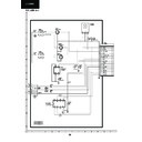
MAJOR ICs INFORMATION
1. IC2001 (RH-IXA665WJN1)
(See note on Source of Documentation Chapter, page 119)
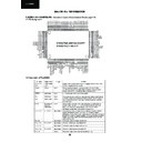
1.1. Pin Assignment.
1.2. Description of Pins IC2001
33
LC-20B6E
P3
0
to P3
7
A
8
to A
15
P4
0
to P4
7
I/O port P3
I/O port P4
This is an 8-bit I/O port equivalent to P0.
These pins output 8 middle-order address bits (A
8
–A
15
).
This is an 8-bit I/O port equivalent to P0.
Input/output
Output
Input/output
Output
Output
Output
CS
0
to CS
3
,
A
16
to A
19
These pins output CS
0
–CS
3
signals and A
16
–A
19
. CS
0
–CS
3
are chip
select signals used to specify an access space. A
16
–A
19
are 4 high-
order address bits.
I/O port P5
P5
0
to P5
7
This is an 8-bit I/O port equivalent to P0. In single-chip mode, P5
7
in
this port outputs a divide-by-8 or divide-by-32 clock of X
IN
or a clock of
the same frequency as X
CIN
as selected by software.
Output
Output
Output
Output
Output
Input
Output
Output
Output
Output
Input
Output
Input
Input
WRL / WR,
WRH / BHE,
RD,
BCLK,
HLDA,
HOLD,
WRH / BHE,
RD,
BCLK,
HLDA,
HOLD,
ALE,
RDY
RDY
Output WRL, WRH (WR and BHE), RD, BCLK, HLDA, and ALE
signals. WRL and WRH, and BHE and WR can be switched using
software control.
■ WRL, WRH, and RD selected
signals. WRL and WRH, and BHE and WR can be switched using
software control.
■ WRL, WRH, and RD selected
With a 16-bit external data bus, data is written to even addresses
when the WRL signal is “L” and to the odd addresses when the WRH
signal is “L”. Data is read when RD is “L”.
■ WR, BHE, and RD selected
Data is written when WR is “L”. Data is read when RD is “L”. Odd
addresses are accessed when BHE is “L”. Use this mode when using
an 8-bit external data bus.
While the input level at the HOLD pin is “L”, the microcomputer is
placed in the hold state. While in the hold state, HLDA outputs a “L”
level. While the input level of the RDY pin is “L”, the microcomputer is in
the ready state. ALE output is indefinite.
Input/output
Signal name
Function
Pin name
I/O type
Input/output
I/O port P6
P6
0
to P6
3,
P6
7
This is an 5-bit I/O port equivalent to P0. When set for input in single-
chip, microprocessor and memory expansion modes, the user can
specify in units of four bits via software whether or not they are tied to a
pull-up resistor. Pins in this port also function as UART0 and multi-
chip, microprocessor and memory expansion modes, the user can
specify in units of four bits via software whether or not they are tied to a
pull-up resistor. Pins in this port also function as UART0 and multi-
master I
2
C-BUS interface 0 I/O pins as selected by software.
Input/output
Input/output
Input/output
I/O port P7
I/O port P9
I/O port P10
P7
0
to P7
7
P9
0
to P9
4
P10
2
to P10
7
This is an 8-bit I/O port equivalent to P6 (P7
0
and P7
1
are N-channel
open-drain output). Pins in this port also function as timers A2 and A3,
UART2, multi-master I
UART2, multi-master I
2
C-BUS interface 0, or H
SYNC
counter I/O pins as
selected by software.
This is an 5-bit I/O port equivalent to P6. Pins in this port also function
as Timer B0 to B2 input pins, D-A converter output pins, or multi-master
as Timer B0 to B2 input pins, D-A converter output pins, or multi-master
I
2
C-BUS interface 1 I/O pins, RXD2, and TXD2 pins. P9
2
can be set
using software to function as the R0 outout pin of digital RGB output.
This is an 6-bit I/O port equivalent to P6. Pins in this port also function
as A-D converter input pins. P10
as A-D converter input pins. P10
5
to
P107
can be set using software to
function as the B2, G2, and R2 outout pins of digital RGB output.
G
Input/output
I/O port P8
P8
2
, P8
3
,
P8
6
, P8
7
P8
2
, P8
3
, P8
6
and P8
7
are I/O ports with the same functions as P6.
Using software, P8
2
and P8
3
can be made to function as the I/O pins for
the input pins for external interrupts. P8
6
and P8
7
can be set using
software to function as the I/O pins for a sub-clock generation circuit,
0
and B
0
output pins of digital RGB output. In this case, connect a
quartz oscillator between P8
6
(X
COUT
pin) and P8
7
(X
CIN
pin).
R, G, B
OSC1/
OSCHLF
OSCHLF
OSC2
CV
IN1
V
HOLD1/
V
HOLD2
HLF1/HLF2
TVSETB
OSD output
Clock for
OSD
OSD
Clock for OSD
I/O for data
slicer
slicer
Test input
Output
Input
Output
Input
Input
Input
These are OSD output pins (Digital/analog outputs selectable).
OSD clock input or filter pin.
This is an OSD clock output pin.
Input composite video signal through a capacitor.
Connect a capacitor between V
HOLD
and Vss.
Connect a filter using of a capacitor and a resistor
between HLF and Vss.
between HLF and Vss.
This is a test input pin. Fix it to “L.”
OUT1, OUT2
These are OSD output pins (digital output).
OSD output
Output
Input/output
CV
IN2
Hsync
Synchronous
signal input for
OSD
signal input for
OSD
Input
This is horizontal synchronous signal pin for OSD.
Vsync
Synchronous
signal input for
OSD
signal input for
OSD
Input
This is vertical synchronous signal pin for OSD.
34
LC-20B6E
2. IC801 (VHITC90203X-1Q)
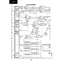
2.1. Block Diagram
Sy
n
c
.
process
Sy
n
c
.
Sepa.
Clock
Gene
rator
HV separator
an
d
sy
nch
ronous
pla
y
back block
42 MHz
Main sy
nc out
Monitor out
Analog
monitor
output
10bit D/A
ITU-R
656
Digital Y
C
bCr
8bit
Digital Y
C
bCr
16
bit
DRAM
F/E block
YCS
Color
Decode
r
Vertical
Enhancer
LTI
sub-
Contrast
Color
Decode
ACC
sub-Color
sub-TIN
T
ITU-R
656
Encoder
ITU-R
601
encoder
Clamp
10bit
A/D
YCS
3-D comb
3D-L comb
A/D block
8bit
A/D
8bit
A/D
8bit
A/D
C
Cb/Cr
R/G/B
SW
C
Cb/B
CR/R
SW
Main-
CVBS/
Y
Main-
CVBS-1/
Y
-1
Main-
CVBS-2/
Y
-2
C
Cb
Cr
R
G
B
ITU-R
656
YCb
Cr 8Bi
t
Y
C
b
C
r 16bit
SW
F/E-I/F block
Y/Cb/
C
r
RGB
YCb
Cr
Matrix
Main screen
processing
I-P
conversion
Motion
adaptive
Scaling
VG
A,
w-VGA,
XG
A
DRAM
I-P conversion and
scaling blo
ck
Subscreen
processing
Scaling
VG
A,
w-VGA,
XG
A
Selector
Main/Sub
User Contr
o
l
Contrast
Brightness
Color
TINT
Y
/C image
quality
correction
block
Sharpness
LTI/CT
I
Vertical
contour
Black
expansion
Y
-g
a
mma
compensation
Relative
phase
Relative
amplitude
YCb
Cr
RG
B
Matrix
Blending
Video
OSD/
TeleTEXT
SW
PC
TeleTEXT
OSD input
interface
C.L.U.T.
OSD block
OSD-d
a
ta/
Y
s
B/E image quality correction bloc
k
RGB image
quality
adjustment
RGB-g
amma
compensation
(C.L.U.
T.
method)
Cut off
Drive
Dither
LCD
interface
2-phase
Digital-RGB
24bit
ITU-R
656
Y
C
b
C
r8bit/
Y
C
b
C
r16bit
input
interface
Subscreen
image
quality
adjustment
sub-
contrast
Sub-
brightness
sub-color
Sub-TIN
T
Input interface
block
Digital RGB
input
interface
R/G/B
Digital-Y
CbC
r
8bit/16bit
Digital-RGB
24bit
35
LC-20B6E
2.2. Pin Functions
Pin Type
Block
Number
of Pins
Pin Name
I/O Type
Description
XO VDD
VDD
Power supply for crystal oscillation block
XO V in
I
D
Input to crystal oscillation block
XO V out
O
D
Output from crystal oscillation block
X’tal 4
XO GND
GND
Ground for crystal oscillation block
Y_BIASAD
A
Bias voltage for 10-bit A/D
YVREFT
A
Reference top voltage for 10-bit A/D
CVBS1 in
I
A
CVBS-1/Y-1 analog video signal input
YVREFM
A
Reference middle voltage for 10-bit A/D
YAD GND
GND
Ground for 10-bit A/D block
CVBS2 in
I
A
CVBS-2/Y-2 analog video signal input
YAD VDD
VDD
Power supply for 10-bit A/D block
10bit A/D
8
YVREFB
A
Reference bottom voltage for 10-bit A/D
C_BIASAD
A
Bias voltage for 8-bit A/D (1)
CVREFT
A
Reference top voltage for 8-bit A/D (1)
C in
I
A
C input
CAD VDD
VDD
Core power supply for 8-bit A/D (1)
Green in
I
A
G input
CVREFB
A
Reference bottom voltage for 8-bit A/D (1)
CAD GND
GND
Core ground for 8-bit A/D (1)
C2_BIASAD
A
Bias voltage for 8-bit A/D (2)
C2VREFT
A
Reference top voltage for 8-bit A/D (2)
Cb in
I
A
Cb input
C2AD VDD
VDD
Core power supply for 8-bit A/D (2)
Blue in
I
A
B input
C2VREFB
A
Reference bottom voltage for 8-bit A/D (1)
C2AD GND
GND
Core ground for 8-bit A/D (2)
C3_BIASAD
A
Bias voltage for 8-bit A/D (3)
C3VREFT
A
Reference top voltage for 8-bit A/D (3)
Cr in
I
A
Cr input
C3AD VDD
VDD
Core power supply for 8-bit A/D (3)
Red in
I
A
R input
C3VREFB
A
Reference bottom voltage for 8-bit A/D
3ch.
8bit A/D
8bit A/D
21
C3AD GND
GND
Core ground for 8-bit A/D (3)
DA VDD1
VDD
Power supply for 10-bit D/A block
DA out1
O
A
Y, Cb, Cr output
DA GND1
GND
Ground for 10-bit D/A block
DABIAS11
A
Bias voltage for 10-bit D/A
DABIAS12
A
Bias voltage for 10-bit D/A
DAVREF1
A
Reference voltage for 10-bit D/A block
DA DVDD1
VDD
Digital power supply for 10-bit D/A block
F/E
10bit D/A
8
DA DVSS1
GND
Digital ground for 10-bit D/A block

