Read Sharp 28JW-73H (serv.man11) Service Manual online
-:+
7'$,&,&
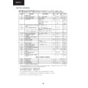
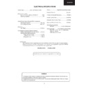
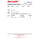
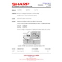
ELECTRICAL CHARACTERISTICS (Refer to the test circuit, V
CC
=
±
14V; R
L
= 8
Ω
; R
S
= 50
Ω
;
R
f
= 12K
Ω
; Demod.. filter L = 60
µ
H, C = 470nF; f = 1KHz; T
amb
= 25°C unless otherwise specified.)
Symbol
Parameter
Test Condition
Min.
Typ.
Max.
Unit
V
S
Supply Range
±
10
±
16
V
I
q
Total Quiescent Current
R
L
=
∞
; NO LC Filter
25
40
mA
V
OS
Output Offset Voltage
Play Condition
–50
+50
mV
P
O
Output Power
THD = 10%
THD = 1%
THD = 1%
8.5
6
10
7
W
W
W
R
L
= 4
Ω
V
CC
=
±
10.5V
THD = 10%
THD = 1%
THD = 1%
10
7
W
W
W
P
d
(*)
Dissipated Power at 1W Output
Power
Power
R
f
= 12K
Ω
P
Ο
= 1W
1
W
P
DMAX
Maximum Dissipated Power
P
Ο
= 10W THD 10%
R
th-j-amb
= 38°C/W (Area 12cm
2
)
1.8
W
η
Efficiency
≡
P
O
P
O
+
P
D
≡
P
O
P
I
(**)
THD 10%
R
R
th-j-amb
= 38°C/W (Area 12cm
2
)
80
85
%
THD
Total Harmonic Distortion
R
L
= 8
Ω
; P
O
= 0.5W
0.1
%
I
max
Overcurrent Protection
Threshold
Threshold
R
L
= 0
3.5
5
A
T
j
Thermal Shut-down Junction
Temperature
Temperature
150
°C
G
V
Closed Loop Gain
29
30
31
dB
e
N
Total Input Noise
A Curve
f = 20Hz to 22KHz
f = 20Hz to 22KHz
7
12
µ
V
µ
V
R
i
Input Resistance
20
30
K
Ω
SVR
Supply Voltage Rejection
f = 100Hz; V
r
= 0.5
46
60
dB
T
r
, T
f
Rising and Falling Time
50
ns
R
DSON
Power Transistor on Resistance
0.4
Ω
F
SW
Switching Frequency
100
120
140
KHz
F
SW_OP
Switching Frequency Operative
Range
Range
100
200
KHz
B
F
Zero Signal Frequency
Constant (***)
Constant (***)
1.4x10
9
Hz
Ω
R
F
Frequency Controller Resistor
Range (****)
Range (****)
7
12
14
K
Ω
MUTE & STAND-BY FUNCTIONS
V
ST-BY
Stand-by range
0.8
V
V
MUTE
Mute Range
1.8
2.5
V
V
PLAY
Play Range (1)
4
V
A
MUTE
Mute Attenuation
60
80
dB
I
qST-BY
Quiescent Current @ Stand-by
3
5
mA
*: The output average power when the amplifier is playing music can be considered roughly 1/10 of the maximum output power. So it is useful
to consider the dissipated power in this condition for thermal dimensioning.
to consider the dissipated power in this condition for thermal dimensioning.
**: P
O
= measured across the load using the following inductor:
COIL 58120 MPPA2 (magnetics) TURNS: 28
∅
1mm
COIL77120 KOOL M
µ
(magnetics) TURNS: 28
∅
1mm
***: The zero-signal switching frequency can be obtained using the following expression: F
SW
= B
F
/R
F
****: The maximum value of R
F
is related to the maximum possible value for the voltage drop on R
F
itself.
(1): For V
12
>5.2V, an input impedance of 10K
Ω
is to be considered.
-:+
063*,&
Fig. 1–1: Simplified functional block diagram of the MSP 34x0G
So
ur
c
e
Se
le
ct
Loud-
SCART1
SCART2
SCART1
SCART2
SCART4
SCART3
MONO
De-
modulator
Headphone
Headphone
I
2
S
Sound
Processing
speaker
Sound
Processing
DAC
DAC
ADC
Loud-
DAC
DAC
ADC
Subwoofer
SCART
DSP
Input
Select
Pre-
processing
SCART
Output
Select
Prescale
Prescale
I
2
S1
I
2
S2
Sound IF1
Sound IF2
speaker
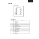
Fig. 4–9: PQFP80 package
65
66
67
68
69
70
71
72
73
74
75
76
77
78
79
80
40
39
38
37
36
35
34
33
32
31
30
29
28
27
26
25
1
2
3
4
56
7
8
9
10 11 12 13 14 15
16 17 18 19 20 21 22 23 24
64 63 62 61 60 59 58 57 56 55 54 53 52 51 50 49 48 47 46 45 44 43 42 41
AVSUP
AVSUP
ANA_IN1+
ANA_IN
−
ANA_IN2+
TESTEN
XTAL_IN
XTAL_OUT
TP
AUD_CL_OUT
NC
NC
D_CTR_I/O_1
D_CTR_I/O_0
ADR_SEL
STANDBYQ
CAPL_M
AHVSUP
CAPL_A
SC1_OUT_L
SC1_OUT_R
VREF1
SC2_OUT_L
SC2_OUT_R
NC
NC
DACM_SUB
NC
DACM_L
DACM_R
VREF2
DACA_L
NC
AVSS
AVSS
MONO_IN
NC
VREFTOP
SC1_IN_R
SC1_IN_L
ASG
NC
SC2_IN_R
SC2_IN_L
ASG
SC3_IN_R
SC3_IN_L
ASG
SC4_IN_R
SC4_IN_L
NC
AGNDC
AHVSS
AHVSS
NC
NC
I2C_CL
I2C_DA
I2S_CL
I2S_WS
I2S_DA_OUT
I2S_DA_IN1
ADR_DA
ADR_WS
ADR_CL
NC
DVSUP
DVSUP
DVSUP
DVSS
DVSS
DVSS
I2S_DA_IN2
NC
NC
NC
RESETQ
NC
NC
DACA_R
MSP 34x0G
-:+
063*,&
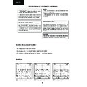
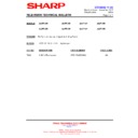
4.6.1. Absolute Maximum Ratings
Stresses beyond those listed in the “Absolute Maximum Ratings” may cause permanent damage to the device. This
is a stress rating only. Functional operation of the device at these or any other conditions beyond those indicated in
the “Recommended Operating Conditions/Characteristics” of this specification is not implied. Exposure to absolute
maximum ratings conditions for extended periods may affect device reliability.
Symbol
Parameter
Pin Name
Min.
Max.
Unit
T
A
Ambient Operating Temperature
−
0
70
°C
T
S
Storage Temperature
−
−40
125
°C
V
SUP1
First Supply Voltage
AHVSUP
−0.3
9.0
V
V
SUP2
Second Supply Voltage
DVSUP
−0.3
6.0
V
V
SUP3
Third Supply Voltage
AVSUP
−0.3
6.0
V
dV
SUP23
Voltage between AVSUP
and DVSUP
and DVSUP
AVSUP,
DVSUP
DVSUP
−0.50.5 V
P
TOT
Power Dissipation
PLCC68
PSDIP64
PSDIP52
PQFP80
PLQFP64
PLCC68
PSDIP64
PSDIP52
PQFP80
PLQFP64
AHVSUP,
DVSUP,
AVSUP
DVSUP,
AVSUP
1200
1300
1200
1000
960
1300
1200
1000
960
mW
mW
mW
mW
mW
mW
mW
mW
mW
V
Idig
Input Voltage, all Digital Inputs
−0.3
V
SUP2
+0.3
V
I
Idig
Input Current, all Digital Pins
−
−20
+20
mA
1)
V
Iana
Input Voltage, all Analog Inputs
SCn_IN_s,
2)
MONO_IN
−0.3
V
SUP1
+0.3
V
I
Iana
Input Current, all Analog Inputs
SCn_IN_s,
2)
MONO_IN
−5
+5mA
1)
I
Oana
Output Current, all SCART Outputs
SCn_OUT_s
2)
3)
,
4)
3)
,
4)
I
Oana
Output Current, all Analog Outputs
except SCART Outputs
except SCART Outputs
DACp_s
2)
3)
3)
I
Cana
Output Current, other pins
connected to capacitors
connected to capacitors
CAPL_p,
2)
AGNDC
3)
3)
1)
positive value means current flowing into the circuit
2)
“n” means “1”, “2”, “3”, or “4”, “s” means “L” or “R”, “p” means “M” or “A”
3)
The analog outputs are short-circuit proof with respect to First Supply Voltage and ground.
4)
Total chip power dissipation must not exceed absolute maximum rating.
-:+
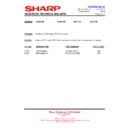
6.7.1. Absolute Maximum Ratings
1)
Refer to Pin Circuits (chapter 6.6. on page 157)
Stresses beyond those listed in the “Absolute Maximum Ratings” may cause permanent damage to the device. This
is a stress rating only. Functional operation of the device at these or any other conditions beyond those indicated in
the “Recommended Operating Conditions/Characteristics” of this specification is not implied. Exposure to absolute
maximum ratings conditions for extended periods may affect device reliability.
is a stress rating only. Functional operation of the device at these or any other conditions beyond those indicated in
the “Recommended Operating Conditions/Characteristics” of this specification is not implied. Exposure to absolute
maximum ratings conditions for extended periods may affect device reliability.
Symbol
Parameter
Pin Name
Min.
Max.
Unit
T
A
Ambient Operating Temperature
−
65
°C
T
S
Storage Temperature
−40
125°C
P
TOT
Total Power Dissipation
−
1400
mW
VSUP
x
Supply Voltage
VSUP
x
−0.3
6
V
V
I
Input Voltage, all Inputs
−0.3
VSUP
x
+0.3
1)
V
V
O
Output Voltage, all Outputs
−0.3
VSUP
x
+0.3
1)
V
V
IO
Input/Output Voltage, all Open Drain Out-
puts
puts
−0.3
6
V
9&7,&
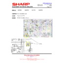
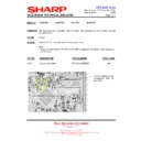
Fig. 1–2: Block diagram of the VCT 38xxA/B (shaded blocks are optional)
The block diagram does not show the additional features of VCT 38xxB.
Video
Front-end
Comb
Filter
Color
Decoder
Display
Processor
Video
Back-end
Panorama
Scaler
4
3
4
12
31
2
I
2
C Master
3 kB
OSD
OSD
96 kB
CPU ROM
TPU
DMA
CPU
24 IO Ports
Watchdog
2 CapCom
2 Timer
15:1 Mux
10-bit ADC
10-bit ADC
8-bit PWM
Audio
3
2
Clock
Oscillator
1 kB
CPU RAM
XTAL1
XTAL2
VIN
AIN
Px
y
ADB, DB, CB
RGBOUT
RGBIN
VE
R
T
PR
OT
HFLB
SE
N
S
E
I
2
C
XR
E
F
HOUT
VR
D
VR
T
SG
N
D
Color, Prio
MSync
I
2
C
VSUPAB
VS
U
PP1
GN
D
P
1
Reset
Logic
RESQ
VS
U
P
S
TEST
GNDAB
VS
U
P
A
F
VS
U
P
D
GNDA
F
GNDD
RS
W
2
GNDM
EW
8
14-bit PWM
2
2
3
CIN
SVM
Vi
d
e
o
GNDS
CLK20
RDY
BE
24
kB
VCT 38xxA/B
AOUT
VSync
VOUT
24 kB ROM
3 kB
OSD RAM
Pict.Improv
16 kB
Text
RAM

