Read Sharp AL-1566 (serv.man15) Service Manual online
AL-1556/1566 ELECTRICAL SECTION 12 - 1
[12] ELECTRICAL SECTION
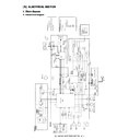
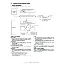
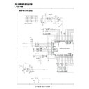
1. Block diagram
A. Overall block diagram
Carriage Unit
CCD PWB
12V
1
2
V
Reg
A5V
3.3V
R
G
8bits (MSB/LSB)
B
SPF M
o
to
r
5V
Speaker
Mechanical Load
FAX only
MPFS,RRS,CPFS1
MCU-PWB
(SPF UNI
T
SGS
,
SRRC,
S
PUS,
SPPS,
4Mb
or 8Mb
(Counter)
MCNT
256Mbx1
o
r 16Mb
3.3V
D[7..0]
RD
CS
INT
Sensor/SW
(Electorical detector/SW/Sensor)
UART
CPU
INTERRUPT
Printer CLK(16.1511MHz)
SPPD
3.3V
CPU I/O
Scanner CLK(48MHz)
32.3022MHz
1
2
MHz
Interlock SW
Cassette detector
X 2
Drum Initial detector
PPD1
POD
A[19
…
1]
OPE PWB
MFD
Duplex Motor
PPD2
D[15
…
0]
SDOD
1Mbit
SPOD
PSL LED
Shifter Motor
Note: Energy-saving 1W correspondence)
8Mbit
8bit
AL-1566 (FAX Model) Only
I2C Bus
8bit
2Kbyte
FAX OPE PWB
Buzzer
Fan Motor (1speed)
Main Motor
Toner Motor
Mirror Motor
Polygon
Motor
AC Code
KRONOS ASIC
(296pin)
CPU
H8S/2321
(19.6608MHz)
LSU
EEPROM
SDRAM
16Mbyte
Reset IC
SRAM
Driver
Flash ROM
AFE(AD9826)
C
D
S
A
G
C
M
P
X
AD
16bits
CCD Driver
CCFL x 2
Lamp
Inverter
HOME
POSITION
SENSOR
CCD
(uPD8861)
CPU CLK(19.6608MHz)
System Reset
SSCG
PMD
Driver
LED Driver
LED
Copier
11
pcs
HC
1
5
1
KEY Matrix
Copier 24pcs
START KEY
POWER SUPPLY
/POFF,HL,PR
FW
3.3V,5VEN,5V,24V
HVU
TC, GRID, MC, BIAS
PMCLK
PSW
KEYIN
SELIN1,2,3
OP-CLK
OP-LATCH
OP-DATA
PSL
MHPS
Driver
Driver
/MMRDY
/MMD
PWM
0 - 24V
HC151
DC-DC
Image BUS(PI-Bus)
Image BUS(PO-Bus)
OA982
SDRAM
Flash ROM
8
8
KEYSCAN1-3
ISP1581
USB2.0
High-speed
P-Bus
LCD
(2 x 20)
FAX/I/F
HC238
(3 to 8 decode)
EEPROM
(CRUM)
LCD E
LCD RS
LCD R/W(TBD)
LCD DB7-4
FAX
Modem / LIU PWB
Driver
LCX574
LASER
KEY Matrix
21 pcs
LED
3 pcs
NIC PCBA
(Internal)
RJ45
(N/W
con-
nector)
Ether Chip
RTL8019AS
FPGA
CPU
uPD703100
FlashROM
1Mbit
SRAM
256kbit
AL-1556/1566 ELECTRICAL SECTION 12 - 2
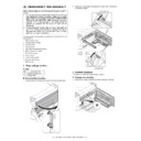
2. Circuit descriptions
A. Main PWB (MCU)
(1) General
The MCU PWB is composed of:
• CPU peripheral section which performs mechanical sequence
control, U/I, and each function job management.
The CPU connects with the ASIC and memory by use of the system
bus and performs jog management and sequence control of the
whole engine.
The CPU connects with the ASIC and memory by use of the system
bus and performs jog management and sequence control of the
whole engine.
• Image process ASIC which performs image process, CCD control,
LSU control, and print control.
• OA982 peripheral section which performs E-Sort and FAX control.
The OA982 performs image data input/output with the ASIC,
SDRAM memory management, and communication with USB2.0
devices.
SDRAM memory management, and communication with USB2.0
devices.
• I/F section for USB2.0 and IEEE1284 control. (For the AL series,
IEEE1284 is not available.)
• Motor control circuit
• Mechanical load, sensor I/O circuit
It performs control and management of the process, the transport
loads, the fusing, the optical, and the operation panel sections for exe-
cuting a series of copy/print/scan operations.
loads, the fusing, the optical, and the operation panel sections for exe-
cuting a series of copy/print/scan operations.
(2) CPU signal table (H8S/2321)
PIN
No.
Signal code
Input/
Output
Operating
1
/CS1
Output
SRAM chip select
2
/CS0
Output
Flash ROM chip select
3
GND
DGND
4
GND
DGND
5
Vcc
CPU3.3V
6
A0
Output
Address bus
7
A1
Output
Address bus
8
A2
Output
Address bus
9
A3
Output
Address bus
10
GND
DGND
11
A4
Output
Address bus
12
A5
Output
Address bus
13
A6
Output
Address bus
14
A7
Output
Address bus
15
A8
Output
Address bus
16
A9
Output
Address bus
17
A10
Output
Address bus
18
A11
Output
Address bus
19
GND
DGND
20
A12
Output
Address bus
21
A13
Output
Address bus
22
A14
Output
Address bus
23
A15
Output
Address bus
24
A16
Output
Address bus
25
A17
Output
Address bus
26
A18
Output
Address bus
27
A19
Output
Address bus
28
GND
DGND
29
A20
Pull-Up
30
PSW
Interruption
level input
level input
Print SW
31
SPPD
Interruption
level input
level input
SPF paper sensor
32
CCD_TG
Interruption
level input
level input
CCD horizontal sync signal
33
MHPS
Interruption
level input
level input
Mirror Home Position
34
/CPUSYNC
Interruption
level input
level input
Horizontal sync (ASIC)
35
GND
DGND
36
GND
DGND
37
FW
Interruption
level input
level input
Zero cross signal
38
ARB_INT
Interruption
level input
level input
ASIC interruption
39
Vcc
CPU3.3V
40
D0
Data I/O
Data bus
41
D1
Data I/O
Data bus
42
D2
Data I/O
Data bus
43
D3
Data I/O
Data bus
44
GND
DGND
45
D4
Data I/O
Data bus
46
D5
Data I/O
Data bus
47
D6
Data I/O
Data bus
48
D7
Data I/O
Data bus
49
D8
Data I/O
Data bus
50
D9
Data I/O
Data bus
51
D10
Data I/O
Data bus
52
D11
Data I/O
Data bus
53
GND
DGND
54
D12
Data I/O
Data bus
55
D13
Data I/O
Data bus
56
D14
Data I/O
Data bus
57
D15
Data I/O
Data bus
58
Vcc
CPU3.3V
59
POFF
Output
Shut off control
60
TxD1
Output
For debug
61
SDA
Output
EEPROM Data bus
62
SCL
Output
EEPROM clock
63
LCDRS
Output
LCD control
64
LCDE
Output
LCD control
65
GND
DGND
66
CS4 (FAX)
Chip select (FAX)
67
GND
DGND
68
GND
DGND
69
RY/BY
Input
Flash Busy signal
70
LCDDB4
Output
LCD control
71
LCDDB5
Output
LCD control
72
BZR
Output
Buzzer signal
73
LCDDB7
Output
LCD control
74
LCDDB6
Output
LCD control
75
Reset OUT1
Output
Reset signal
76
DMT0
Output
Duplex Motor signal
77
DMT1
Output
Duplex Motor signal
78
DMT2
Output
Duplex Motor signal
79
DMT3
Output
Duplex Motor signal
80
WDTOVF
Output
NC Pull-Up
81
/RES
Input
Reset
82
NMI
Output
NC Pull-Up
83
STBY
Output
NC Pull-Up
84
Vcc
CPU3.3V
85
XTAL
Input
Clock
86
EXTAL
Output
Clock
87
GND
DGND
88
CPUCLK
Output
NC
89
Vcc
CPU3.3V
90
PRINTST
Output
Print start signal
91
/RD
Output
Read signal
92
/HWR
Output
Write signal (High address)
93
/LWR
Output
Write signal (Low address)
94
SELIN3
Output
HC151 select signal
95
SELIN2
Output
HC151 select signal
96
SELIN1
Output
HC151 select signal
97
ESSTS
Output
E-sort control
98
ESCMD
Input
E-sort control
99
GND
DGND
100
GND
DGND
101
ESSRDY
Input
E-sort control
102
ESCRDY
Output
E-sort control
103
AVcc
CPU3.3V
104
Vref
CPU3.3V
105
RTH
Analog
input
input
Fusing thermistor
PIN
No.
Signal code
Input/
Output
Operating
AL-1556/1566 ELECTRICAL SECTION 12 - 3
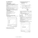
(3) Image process ASIC (HG73C114HF)
a. General
The ASIC is composed of the three blocks: the image process block,
the print control block, and the I/F block.
the print control block, and the I/F block.
Image process section
According to the operation mode set by the register set value, the
image data from the CCD PWB are placed under shading, AE pro-
cess, input gamma process, area separation, filter process, resolu-
tion conversion, zoom process, output gamma process, and binary
coding.
image data from the CCD PWB are placed under shading, AE pro-
cess, input gamma process, area separation, filter process, resolu-
tion conversion, zoom process, output gamma process, and binary
coding.
Print control section
During copying, image-processed data are outputted to the LSU at
the timing of LSU writing.
the timing of LSU writing.
I/F section
This section performs DRUM control as image data buffer, image
data send/receive with the OA982, and data send/receive with the
IEEE1284 I/F.
data send/receive with the OA982, and data send/receive with the
IEEE1284 I/F.
106
ESPAGE
Input
E-sort control
107
SIN1
Input
HC151 select detection
108
SIN2
Input
HC151 select detection
109
SIN3
Input
HC151 select detection
110
Pull up
111
KEY IN
Input
NC
112
MSUST1
Input
NC
113
Avss
DGND
114
GND
DGND
115
/SCANSP
Output
Scan STOP signal
116
/SCANST
Output
Scan START signal
117
/TRANSST
Output
ASIC transfer signal
118
PMCLK
Output
Polygon clock
119
SPMT3
Output
SPF motor signal
120
SPMT2
Output
SPF motor signal
121
SPMT1
Output
SPF motor signal
122
SPMT0
Output
SPF motor signal
123
GND
DGND
124
GND
DGND
125
Vcc
CPU3.3V
126
PSL
Output
Power save LED control
127
/CS3
Output
Chip select signal
128
/CS2
Output
ASIC chip select
PIN
No.
Signal code
Input/
Output
Operating
nCS2
nRD
PORT1OUT[15..0]
nLWR
PORT2OUT[10..0]
A[9..1]
D[15..0]
OPE-LATCH
LED Driver
OPE-DATA
to OPU-PWB
nRESET
Control
OPE-CLK
JTAG
TONER MOTOR
TMCLK,TMEN
to TONER MOTOR DRIVER
Control
TM,TM-
to SDRAM
64Mb or 128Mb
64Mb or 128Mb
CCD-RS,CCD-CK1,CCD-CK2
to CCD(SCAN UNIT)
(Op.400MByte)
CCD-CP,CCD-SHR
bsmp,vsmp,mclk,OEB
afesen,afesck,afesdi
to AFE(SCAN UNIT)
to USB I/F
AFE-DB[7..0]
to IEEE1284 I/F
MIRCNT,MTR-Y1,MTR-PH-1,MTR-I01,MTR-I11,MTR-I21
MTR-Y2,MTR-PH-2,MTR-I02,MTR-I12,MTR-I22
to MIRROR MOTOR DRIVER
SYNC
to LSU-PWB
LD
to CCFL(Scan UNIT)
LEND
CL
CPUSYNC
I/O PORT
CPU BUS
I/F
AL-1556/1566 ELECTRICAL SECTION 12 - 4
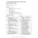
b. ASIC (Signal table)
PIN
No.
Signal Name
IN/OUT Connected to
Description
1
cpudata7
IN/OUT CPU
CPU data bus
2
cpudata6
IN/OUT CPU
CPU data bus
3
cpudata5
IN/OUT CPU
CPU data bus
4
cpudata4
IN/OUT CPU
CPU data bus
5
VCC_AC
Power
6
cpudata3
IN/OUT CPU
CPU data bus
7
cpudata2
IN/OUT CPU
CPU data bus
8
cpudata1
IN/OUT CPU
CPU data bus
9
cpudata0
IN/OUT CPU
CPU data bus
10
GND_AC
Power
11
mircnt
OUT
Buffer IC
SPF scanner select
signal
signal
12
cpusync
OUT
CPU
CPU SYNC signal
13
mem_intr
Not used
14
arb_intr
OUT
CPU
INTR signal
15
VCC_core
Power
16
cpu_ad8
IN
CPU
CPU address bus
17
cpu_ad7
IN
CPU
CPU address bus
18
cpu_ad6
IN
CPU
CPU address bus
19
cpu_ad5
IN
CPU
CPU address bus
20
GND_core
Power
21
ram_clk_in
IN
ASIC
SDRAM clock on the
board
board
22
cpu_ad4
IN
CPU
CPU address bus
23
cpu_ad3
IN
CPU
CPU address bus
24
cpu_ad2
IN
CPU
CPU address bus
25
cpu_ad1
IN
CPU
CPU address bus
26
cpu_ad0
IN
CPU
CPU address bus
27
xcpucs
IN
CPU
CS signal
28
sfclk
IN
Oscillator
Clock
29
GND_core
Power
30
xcpuwr
IN
CPU
CPU write signal
31
xcpurd
IN
CPU
CPU read signal
32
nrst
IN
SYSTEM
RESET
RESET
SYSTEM RESET
33
VCC_core
Power
34
pfclk2
IN
Not used
35
clock_sw
IN
Pull up
36
GND_core
Power
37
pfclk1_xout
OUT
X-tal units
VIDEO clock
38
pfclk1
IN
X-tal units
VIDEO clock
39
VSSPLL2
Pull up
40
VDDPLL2
Pull up
41
VSS2
Pull up
42
VDDI2
Pull up
43
tm2_15m
Pull up
44
xsync
IN
LSU
Horizontal sync
signal from LSU
(/SYNC)
signal from LSU
(/SYNC)
45
GND_AC
Power
46
xld
OUT
LSU
Laser drive signal
47
xlend
OUT
LSU
Laser APC signal
48
VCC_AC
Power
49
mmd
OUT
Tr array IC
Main motor control
signal. "H": Main
motor ON
signal. "H": Main
motor ON
50
pmd
OUT
I/O
Polygon motor drive
51
tc
OUT
Tr array IC
Transfer charger
control signal. "H":ON
control signal. "H":ON
52
gridl
OUT
Tr array IC
Main charger grid
control signal. "H": L
output
control signal. "H": L
output
53
mc
OUT
Tr array IC
Main charger control
signal. "H": ON
signal. "H": ON
54
bias
OUT
I/O
HV bias drive
55
NC
OUT
I/O
Not used
56
vfmcnt
OUT
Tr array IC
Ventilation fan
rotation speed control
signal. "H": High
speed, "L": Low
speed
rotation speed control
signal. "H": High
speed, "L": Low
speed
57
VCC_core
Power
58
vfm
OUT
Tr array IC
Ventilation fan control
signal. "H": Fan ON
signal. "H": Fan ON
59
/FPOFF
OUT
I/O
FAX poff signal
60
GND_core
Power
61
DEV DIR
OUT
I/O
CRUM bus control
62
spfclh
OUT
Tr array IC
SPF/RSPF resist
roller clutch control
signal "H":ON
roller clutch control
signal "H":ON
63
spfrsol
OUT
Tr array IC
SPF/RSPF document
feed solenoid control
signal "H":ON
feed solenoid control
signal "H":ON
64
spfgsol
OUT
Tr array IC
SPF/RSPF gate
solenoid control
signal "H":ON
solenoid control
signal "H":ON
65
spfpsol
OUT
Tr array IC
SPF/RSPF document
transport solenoid
control signal "H":ON
transport solenoid
control signal "H":ON
66
VCC_core
Power
67
bias
OUT
Tr array IC
DV bias control
signal. "H":ON
signal. "H":ON
68
lden
OUT
Tr array IC
Laser circuit control
signal. "H": Laser
circuit ON
signal. "H": Laser
circuit ON
69
GND_AC
Power
70
MRPS1
OUT
I/O
SPF current control
71
MRPS2
OUT
I/O
SPF current control
72
MRPS3
OUT
I/O
SPF current control
73
CPFS1
OUT
I/O
1st cassette pick up
solenoid
solenoid
74
VCC_AC
Power
75
CPFS2
OUT
I/O
2nd cassette pick up
solenoid
solenoid
76
pr
OUT
I/O
Power relay control
77
hl
OUT
Tr array IC
Heater lamp control
signal. "H":ON
signal. "H":ON
78
GND_core
Power
79
MPFS
OUT
I/O
Multi-bypass solenoid
80
miron
OUT
Buffer IC
SPF scanner select
signal
signal
81
spfon
OUT
Buffer IC
SPF ON signal
82
KEYSC1
OUT
I/O
Key sense control
83
KEYSC2
OUT
I/O
Key sense control
84
KEYSC3
OUT
I/O
Key sense control
85
IMC ready
OUT
I/O
IMC control
86
VCC_core
Power
87
tmx
OUT
Buffer IC
Toner motor control
signal
signal
88
tm
OUT
Buffer IC
Toner motor control
signal
signal
89
op_data
OUT
Tr array IC
Operation circuit data
signal
signal
90
ope_latch
OUT
Tr array IC
Operation circuit latch
signal. Data take-in at
"L"
signal. Data take-in at
"L"
91
GND_AC
Power
PIN
No.
Signal Name
IN/OUT Connected to
Description

