Read Sharp LL-T1811W (serv.man3) Service Manual online
LL-T1811W
3 – 1
No
Yes
No
Yes
No
Yes
No
Yes
No
Yes
No
Yes
No
Yes
No
Yes
No
No
Yes
No
Yes
No
Yes
No
Yes
No
Yes
No
Yes
No
Yes
Yes
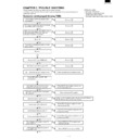
CHAPTER 3. TROUBLE SHOOTING
Screen is not displayed (Analog RGB)
Check whether the following cables are connected correctly.
In addition, check whether the PCs video mode is properly set to the signal timing which
meets this machine.
In addition, check whether the PCs video mode is properly set to the signal timing which
meets this machine.
Attached cables
* Dedicated AC adapter
* Dedicated analog signal cable
(RGB cable, DVI-A cable)
* Dedicated digital signal cable (DVI-D cable)
* Dedicated AC adapter
* Dedicated analog signal cable
(RGB cable, DVI-A cable)
* Dedicated digital signal cable (DVI-D cable)
LED comes on when the power button
is pressed?
is pressed?
1
Perform
LED color changes from green to orange
when RGB cable is removed?
when RGB cable is removed?
B/L is lit?
The screen is displayed properly in each
video mode?
video mode?
No error.
Output of 5 V (main PWB L4)?
Q8 (1st pin) and R40 output 3 V?
LD11 and CN2 (2nd pin) output 1.9 V?
Check Q8 and its surrounding circuits.
Check SW cable and SW PWB
connections.
connections.
Input signal port is the one to which
analog signal cable is connected?
analog signal cable is connected?
Press INPUT key to switch over to the
correct input signal port.
correct input signal port.
DC+12 V is outputted from dedicated
AC adapter?
AC adapter?
Check dedicated AC adapter.
Test terminal LD1 is DC+12 V?
Check DC+12 V power supply line and DC jack PWBs F1,
F2, D1, D2 and their surrounding circuits.
F2, D1, D2 and their surrounding circuits.
Test terminal LD7 is DC+5 V?
Check DC+5 V power supply line and
circuits around IC2.
circuits around IC2.
Test terminal LD6 is DC+3.3 V?
Check DC+3.3 V power supply line and
circuits around IC1.
circuits around IC1.
Test terminal LD8 is DC+2.5 V?
Check DC+2.5 V power supply line and
circuits around IC3.
circuits around IC3.
The voltage at both ends of fuse F3
is DC+12.0 V?
is DC+12.0 V?
Check POWER_CTRL2 signal and
areas around Q4.
areas around Q4.
+ side (parts mounted) of C202 is in
L level (DC+ V)?
L level (DC+ V)?
Check RESET circuit around IC32.
LED color stays green when RGB cable is
connected again?(The color does not
change from green to orange.)
connected again?(The color does not
change from green to orange.)
1
Perform
2
Perform
3
Perform
4
Perform
2
Perform
2
Perform
1
2
LL-T1811W
3 – 2
Yes
Yes
Yes
Yes
Yes
Yes
Yes
Yes
Yes
Yes
Yes
Yes
Yes
Yes
Yes
Yes
No
No
No
No
No
No
No
No
No
No
No
No
No
No
No
No
No
No
3
2
Yes
Yes
continued from
+ side of C28 is DC+5 V?
Check areas around L10.
Test terminal LD21 changes its level when
POWER switch is turned on and off?
POWER switch is turned on and off?
Check MAINPW signal and areas
around CN5.
around CN5.
The output (connected to R35) of Q12
is in H level )DC+5 V)?
is in H level )DC+5 V)?
Check circuits around Q12.
21st pin of IC24 oscillates?
Check IC24 and clock circuit around X1.
C139-side terminal of X2 oscillates?
Check IC6 and clock circuit around X2.
Signal waveforms of test terminals LD58,
LD59 (LD51, LD52) are normal?
LD59 (LD51, LD52) are normal?
Check analog signal cable and
CN8 (CN6).
CN8 (CN6).
Signal waveform of test terminal
LD64 (LD65) is normal?
LD64 (LD65) is normal?
Check circuits around IC19 and IC33.
Signal waveforms of test terminals LD66
and LD67 are normal?
and LD67 are normal?
Check circuits around IC20.
Signal waveforms of test terminals LD24
and LD25 are normal?
and LD25 are normal?
Signal waveforms of test terminals LD22
and LD23 are normal?
and LD23 are normal?
Waveform at IC6 side is normal when
R70/R71 are removed?
R70/R71 are removed?
Replace IC6 with a new one.
Check DCLK and DEN lines.
Waveforms of FL1 FL4 are normal?
Waveform becomes normal when
LCD module is removed?
LCD module is removed?
Check areas around CN3.
Replace LCD module with a new one.
Signal waveforms of CN3s 66th, 70th,
65th, and 69th pins are normal?
65th, and 69th pins are normal?
Check areas around CN3.
Replace LCD module with a new one.
CN3 and CN4 1st and 2nd pins on
DC jack PWB are DC+12 V?
DC jack PWB are DC+12 V?
Check DC+12 V power supply line and
fuse F2.
fuse F2.
Test terminal LD5 is DC+5 V?
Check Q1, Q2, Q11, Q20 and main PWB
and DC jack PWB around CN2.
and DC jack PWB around CN2.
Test terminals LD3 and LD4 are less
than DC+1.0 V?
than DC+1.0 V?
Check main PWB and DC jack PWB
around IC5.
around IC5.
Replace inverter PWB unit with a new one.
Check lamp inside LCD module.
Check microprocessor circuit/GM5020.
5
Perform
CN2s 1st and 2nd pins on inverter PWB unit are about
750 Vrms?
(Use caution not to get electric shock accident. Use high-
voltage probe (more than 100:1) for measuring voltage.)
750 Vrms?
(Use caution not to get electric shock accident. Use high-
voltage probe (more than 100:1) for measuring voltage.)
LL-T1811W
3 – 3
Yes
Yes
Yes
No
No
No
No
No
No
No
No
No
No
No
No
No
No
No
Yes
Yes
Yes
Yes
Yes
Yes
Yes
4
Yes
Yes
Yes
Yes
Yes
Yes
Yes
Yes
No
No
Yes
Check DC+5V power supply line and
circuits around IC2.
circuits around IC2.
Test terminal LD6 is DC+3.3 V?
Check DC+3.3 power supply line and
circuits around IC1.
circuits around IC1.
Test terminal LD8 is DC+2.5 V?
Check DC+2.5 V power supply line and
circuits around IC3.
circuits around IC3.
The entire LCD screen is white?
Clocks (FL3, FL4) and DE FL1, FL2)
signal outputs are normal?
signal outputs are normal?
Check CN3 and LCD module.
The entire LCD screen is black?
The voltage at both ends of fuse F3 is
DC+12.0 V?
DC+12.0 V?
Check POWER CTRL2 signal and
areas around Q4.
areas around Q4.
+ side of C28 is DC+5 V?
Check areas around L10.
Check circuits around X1, X2 and IC24.
The size of LCD screen is abnormal?
ADJUSTMENT and MODE SELECT are
set properly?
set properly?
Adjust according to screen adjustment
procedure”.
procedure”.
Check circuits around X1, X2, IC24 and
C22.
C22.
LCD screen jitters or flickers?
ADJUSTMENT and MODE SELECT
are set properly?
are set properly?
Adjust according to screen adjustment
procedure”.
procedure”.
Check circuits around IC19, IC20, IC33.
LCD screen colors are abnormal?
GAIN CONTROL and WHITE BALANCE
are set properly?
are set properly?
Adjust according to “Screen adjustment
procedure”.
procedure”.
Check circuits around IC27.
Abnormal area moves when
BRIGHT/CONTRAST is changed by
gradation pattern?
BRIGHT/CONTRAST is changed by
gradation pattern?
Display RGB color gradation out of
FL1-FL12 output data lines. Check the
line corresponding to the abnormal color.
FL1-FL12 output data lines. Check the
line corresponding to the abnormal color.
Check circuits around IC10, Ic11, and
IC12.
IC12.
Adjustment settings are stored after
display screen is adjusted?
display screen is adjusted?
Check circuits around IC4 and Ic24.
Input is changed over properly?
Check circuits around IC27.
No error.
2
Perform
Test terminal LD7 is DC+5V?
Analog color signal output is normal?(IC6
side terminals of C153, C156 and C161)
side terminals of C153, C156 and C161)
LL-T1811W
3 – 4
Yes
Yes
Yes
Yes
Yes
Yes
Yes
No
No
No
No
No
No
No
5
Yes
No
No
+ side (parts not mounted) of C202 is in
L level (DC+ 0 V)?
L level (DC+ 0 V)?
Check RESET circuit around IC32.
Output (connected with R35) of Q12 is in
H level (DC+5V)?
H level (DC+5V)?
Check circuits around Q12.
44th pin of IC24, 20th pin of IC25, and
32nd pin of IC7 are DC+5 V?
32nd pin of IC7 are DC+5 V?
Check abnormal power supply line.
Signal waveform appears at data address
bus of IC24, IC25 and IC7?
bus of IC24, IC25 and IC7?
Check circuits around IC24, IC25 and
IC7.
IC7.
Signal waveform is generated at RN2,
R30, R31?
R30, R31?
Check RN2, R30, R31 (IC24 and IC6
control line).
control line).
Check IC6.
PC screen is not displayed (digital DVI)
Display is normal in analog input?
Check with analog input.
DC+5V is inputted to 14th pin of CN6?
Check CN6 and signal source.
Signal level at CN6s 1st, 2nd, 9th, 10th,
17th, 18th, 23rd, 24th pins changes?
17th, 18th, 23rd, 24th pins changes?
IC6 is defective.
Waveform at IC26s 5th and 6th pins
changes normally when resolution is
changed?
changes normally when resolution is
changed?
Check circuits around IC30.
Waveform at IC14s 5th and 12th pins
changes normally when resolution is
changed?
changes normally when resolution is
changed?
Check circuits around IC14.
IC6 is defective.
Yes
No

