Read Sharp SD-CX1 (serv.man10) Service Manual online
– 69 –
SD-CX1H
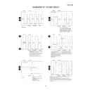
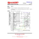
WAVEFORMS OF 1-BIT AMP. CIRCUIT
T
2
1
2.00V/div
500ns/div
194.545465
µ
s
520mV
2.00V/div
AD IC Output
+ Side
- Side
5V
Amplitude
from 0 to 5 V
from 0 to 5 V
1
2
2
2
1
2.00V/div
500ns/div
194.545465
µ
s
-12.30V
2.00V/div
AD IC NF IN
In partial pressure OUT, 4 to 7 V amplitude
of GND reference is observed.
In IC of 75 kohms, the reference is 2.5 V
because of VREF. Due to imaginary GND
of operational amplifier inside IC, the
waveform cannot be monitored.
This waveform is partial pressure OUT.
of GND reference is observed.
In IC of 75 kohms, the reference is 2.5 V
because of VREF. Due to imaginary GND
of operational amplifier inside IC, the
waveform cannot be monitored.
This waveform is partial pressure OUT.
3
4
T
2.00V/div
50.0ns/div
0.0s
-12.30V
2.00V/div
LEVEL SHIFT OUT
DEAD TIME
ZOOM UP
Dead time is generated by level
shift input.
Leading edge is delayed at CR,
passing R at DI.
Set value: 20 -25 nsec
shift input.
Leading edge is delayed at CR,
passing R at DI.
Set value: 20 -25 nsec
5
6
6
T
2.00V/div
500ns/div
194.545465
µ
s
-12.47V
2.00V/div
POWER SUPPLY
LEVEL SHIFT OUT
5V
Waveform after level shift
On the reference side, 5 V amplitude
is observed at + 2 V (negative supply
voltage), corresponding to VINH and
VINL of gate driver during 9 V operation.
(Approx. 0.8 VCC and 0.2 VSS)
On the reference side, 5 V amplitude
is observed at + 2 V (negative supply
voltage), corresponding to VINH and
VINL of gate driver during 9 V operation.
(Approx. 0.8 VCC and 0.2 VSS)
7
8
8
FET is based on the negative
supply voltage; the gate voltage
of the LOW side FET operates
with the negative power and + 9 V.
supply voltage; the gate voltage
of the LOW side FET operates
with the negative power and + 9 V.
To make HIGH SIDE FET
completely on, the positive
supply voltage of + 4.5 V or over
is required. At the bootstrap, the
gate drive voltage is generated;
the HIGH side is driven between
(positive power) + 6 V and the
negative power.
completely on, the positive
supply voltage of + 4.5 V or over
is required. At the bootstrap, the
gate drive voltage is generated;
the HIGH side is driven between
(positive power) + 6 V and the
negative power.
T
2
1
10.0V/div
500ns/div
194.545465
µ
s
-12.3V
10.0V/div
HIGH SIDE OUT
LOW SIDE OUT
GATE DRIVE OUT
9
10
T
10.0V/div
500ns/div
194.545465
µ
s
-12.3V
10.0V/div
+SIDE
+FETOUT
- SIDE
Waveforms before low-pass filters at both ends of the speaker
H-bridge may be considered as BTL.
However, here and at the gate drive, dead time is not observed;
since bootstrap operates based on output, DEAD TIME part is in floating
condition. The waveform on the HI GH side shows that only the booted
voltage lowers.
H-bridge may be considered as BTL.
However, here and at the gate drive, dead time is not observed;
since bootstrap operates based on output, DEAD TIME part is in floating
condition. The waveform on the HI GH side shows that only the booted
voltage lowers.
2
1
11
12
12
SD-CX1H
– 70 –
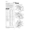
WAVEFORMS OF MD CIRCUIT
POWER ON
TOC READ (Low reflection disc)
TOC READ (Low reflection disc)
TOC READ (Low reflection disc)
PLAY (Low reflection disc)
PLAY (Low reflection disc)
TOC READ (High reflection disc)
TOC READ (High reflection disc)
TOC READ(High reflection disc)
STOP ---> PLAY
TP1518
(RESET)
TP1800
(3.2V)
TP1511
(PCONT0)
TP1212
(FEMON)
TP1422
(DSENSE)
TP1420
(FOK)
TP1201
(EFMMON)
TP1135
(ADIPO)
TP1122
(F+)
TP1207
(TEMON)
TP1603
(SP+)
TP1602
(SP-)
TP1122
(F+)
TP1122
(F+)
TP1207
(TEMON)
TP1603
(SP+)
TP1602
(SP-)
1
2
3
4
4
6
10
11
4
6
10
11
4
5
12
13
14
15
5
6
7
4
5
6
7
4
6
8
9
4
6
8
9
TP1122
(F+)
TP1212
(FEMON)
TP1207
(TEMON)
TP1451
(ADJUST)
TP1122
(F+)
TP1212
(FEMON)
TP1207
(TEMON)
TP1451
(ADJUST)
TP1122
(F+)
TP1207
(TEMON)
TP1601
(SLD+)
TP1600
(SLD-)
TP1122
(F+)
TP1207
(TEMON)
TP1601
(SLD+)
TP1600
(SLD-)
– 71 –
SD-CX1H
REC
Analog REC
Digital REC
Double speed REC
PLAY
PLAY(1kHz 0dB)
PLAY
TP1201
(EFMMON)
TP1201
(EFMMON)
TP1530
(CDLRCK)
TP1515
(DIGIN)
TP1533
(CDDATA)
TP1524
(L OUT)
TP1526
(R OUT)
TP1531
(CDBCK)
TP1207
(TEMON)
TP1207
(TEMON)
TP1121
(T+)
TP1421
(CIN)
TP1121
(T+)
TP1421
(CIN)
72
IC1201
(DFCK)
72
IC1201
(DFCK)
TP1300
(REC HEAD)
TP1302
(EFMO)
TP1105
(LDVAL)
TP1113
(R/P)
71
IC1201
(BCLK)
3
IC1202
(WE)
17
IC1202
(CAS)
1
IC1202
(I/01)
6
IC1202
(A0)
70
IC1201
(LRCK)
74
IC1201
(DADATA)
71
IC1201
(BCLK)
70
IC1201
(LRCK)
73
IC1201
(ADDATA)
PLAY (Low reflection disc)
PLAY (High reflection disc)
14
28
29
30
31
18
32
20
21
33
34
35
36
6
16
17
14
6
16
17
18
19
20
21
22
23
24
25
26
27
SD-CX1H
– 72 –
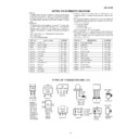
WAVEFORMS OF CD CIRCUIT
T
IC2 11pin
Stopped
CH1=200mV
2000/09/18 16:56:26
DC 10:1
5ms/div
(5ms/div)
NORM:200kS/s
1
=Record Length=
Smoothing : ON
CH1 : 0.000V
CH2 : 0.00V
CH2 : 0.00V
Main : 10K
Zoom : 4K
Zoom : 4K
Mode : AUTO
Type : EDGE CH1
Delay : 102.3ns
Hold off : MINIMUM
Type : EDGE CH1
Delay : 102.3ns
Hold off : MINIMUM
CH3 : 0.00V
CH4 : 0.00V
CH4 : 0.00V
BW : 20MHz
=Trigger=
=Filter=
VAR
CH1 V/DIV
CAL
=Offset=
CH1
V/DIV
200mV
V/DIV
200mV
T
Disc playback
When there is no
wound in the disc.
wound in the disc.
1
Tracking error
TEO
T
TEO
Stopped
CH1=1V
2000/09/18 16:55:04
DC 10:1
5ms/div
(5ms/div)
NORM:200kS/s
1
=Record Length=
Smoothing : ON
CH1 : 0.00V
CH2 : 0.00V
CH2 : 0.00V
Main : 10K
Zoom : 4K
Zoom : 4K
Mode : AUTO
Type : EDGE CH1
Delay : 102.3ns
Hold off : MINIMUM
Type : EDGE CH1
Delay : 102.3ns
Hold off : MINIMUM
CH3 : 0.00V
CH4 : 0.00V
CH4 : 0.00V
BW : 20MHz
=Trigger=
=Filter=
VAR
CH1 V/DIV
CAL
=Offset=
CH1
V/DIV
1V
V/DIV
1V
T
By the
test mode 3
test mode 3
1
Tracking
IC2 11pin
T
TEO
RFRP
Stopped
CH1=1V
2000/09/18 17:01:23
DC 10:1
CH2=1V
DC 10:1
2ms/div
(2ms/div)
NORM:500kS/s
1
2
=Record Length=
Smoothing : ON
CH1 : 0.00V
CH2 : 0.00V
CH2 : 0.00V
Main : 10K
Zoom : 5K
Zoom : 5K
Mode : SINGLE
Type : EDGE CH1
Delay : 102.3ns
Hold off : MINIMUM
Type : EDGE CH1
Delay : 102.3ns
Hold off : MINIMUM
CH3 : 0.00V
CH4 : 0.00V
CH4 : 0.00V
BW : 20MHz
=Trigger=
=Filter=
CH2
CH3
CH4
EXT
LINE
=Offset=
CH1
Level
0.54V
Level
0.54V
T
Track jump
CH1
1
During the tracking jump TEO, RFRP
2
IC2 11pin
IC2 17pin
T
IC2 15
pin
IC1 4 pin
IC1 3 pin
Stopped
CH1=500mV
2000/09/18 15:29:21
DC 10:1
CH2=2V
DC 10:1
CH3=2V
DC 10:1
2ms/div
(2ms/div)
NORM:500kS/s
1
2
3
=Record Length=
Smoothing : ON
CH1 : 0.000V
CH2 : 0.00V
CH2 : 0.00V
Main : 10K
Zoom : 5K
Zoom : 5K
Mode : SINGLE
Type : EDGE CH2
Delay : 102.3ns
Hold off : MINIMUM
Type : EDGE CH2
Delay : 102.3ns
Hold off : MINIMUM
CH3 : 0.00V
CH4 : 0.00V
CH4 : 0.00V
BW : 20MHz
=Trigger=
=Filter=
CH1
CH3
CH4
EXT
LINE
=Offset=
CH2
Level
2.48V
Level
2.48V
T
When a cap was
closed, disc,
dovetail
closed, disc,
dovetail
CH2
3
4
5
Focus servo on
FEO
FO+
FO-
T
RFGO
Stopped
CH1=500mV
2000/09/18 14:55:22
DC 10:1
500ms/div
(500ms/div)
NORM:200kS/s
1
=Record Length=
Smoothing : ON
CH1 : 0.000V
CH2 : 0.00V
CH2 : 0.00V
Main : 1K
Zoom : 400
Zoom : 400
Mode : SINGLE
Type : EDGE CH1
Delay : 102.3ns
Hold off : MINIMUM
Type : EDGE CH1
Delay : 102.3ns
Hold off : MINIMUM
CH3 : 0.000V
CH4 : 0.00V
CH4 : 0.00V
BW : 20MHz
=Trigger=
=Filter=
Format
BMP
FileName
AutoFile
ON
OFF
To
TopMenu
TopMenu
=Offset=
Disc playback
T
6
RF
IC2 19 pin
T
DMO
RFDC
RFRP
Stopped
CH1=1V
2000/09/18 16:45:07
DC 10:1
CH2=1V
DC 10:1
CH3=1V
DC 10:1
500ms/div
(500ms/div)
NORM:2kS/s
1
2
3
=Record Length=
Smoothing : ON
CH1 : 0.00V
CH2 : 0.00V
CH2 : 0.00V
Main : 10K
Zoom : 4K
Zoom : 4K
Mode : SINGLE
Type : EDGE CH1
Delay : 102.3ns
Hold off : MINIMUM
Type : EDGE CH1
Delay : 102.3ns
Hold off : MINIMUM
CH3 : 0.00V
CH4 : 0.00V
CH4 : 0.00V
BW : 20MHz
=Trigger=
=Filter=
=Offset=
T
CD test 2->3
upgrade
upgrade
CH3
V/DIV
1V
V/DIV
1V
7
Disc motor and CD related signal
8
2
IC3 41pin
IC2 12pin
IC2 17pin

