Read Sharp SD-AT50H (serv.man17) Service Manual online
SD-AT50H
– 44 –
FUNCTION TABLE OF IC
IC101 VHiCS493264-1: DSP (CS493264) (1/3)
1
VD1
Input
Digital positive supplies. Norminally + 2.5 V.
2
DGND1
—
Digital ground.
3
AUDATA3, XMT958
Output
CMOS level output that contains a biphase-mark encoded (S/PDIF) or I
2
S or Left
Justified digital audio data which is capable of carrying two channels of PCM
digital audio or an IEC61937 compressed-data interface.
Note: Outputting of IEC61937 is only available for certain broadcast-based
digital audio or an IEC61937 compressed-data interface.
Note: Outputting of IEC61937 is only available for certain broadcast-based
application codes which run on the CS4931X family or CS49330 device.
This output typically connects to the input of an RS-422 transmitter or to the
input of an optical transmitter.
input of an optical transmitter.
4
WR, DS, EMWR, GPIO10
Input
In Intel parallel host mode, this pin serves as the active-low data-write-input
strobe. In Motorola parallel host mode, this pin serves as the active-low data-
strobe-input signal. In serial host mode, this pin can serve as the external-
memory active-low write-enable output signal. Also in serial host mode, this pin
can serve as a general purpose input or output bit.
strobe. In Motorola parallel host mode, this pin serves as the active-low data-
strobe-input signal. In serial host mode, this pin can serve as the external-
memory active-low write-enable output signal. Also in serial host mode, this pin
can serve as a general purpose input or output bit.
5
RD, R/W, EMOE, GPIO11
Input
In Intel parallel host mode, this pin serves as the active-low data bus enable
input. In Motorola parallel host mode, this pin serves as the read-high/write-low
control input signal. In serial host mode, this pin can serve as the external
memory active-low data-enable output signal. Also in serial host mode, this pin
can serve as a general purpose input or output bit.
input. In Motorola parallel host mode, this pin serves as the read-high/write-low
control input signal. In serial host mode, this pin can serve as the external
memory active-low data-enable output signal. Also in serial host mode, this pin
can serve as a general purpose input or output bit.
6
A1, SCDIN
Input
In parallel host mode, this pin serves as one of two address input pins used to
select one of four parallel registers. In SPI serial host mode, this pin serves as
the data input.
select one of four parallel registers. In SPI serial host mode, this pin serves as
the data input.
7
A0, SCCLK
Input
In parallel host mode, this pin serves as one of two address input pins used to
select one four parallel registers. In serial host mode, this pin serves as the serial
control clock signal, specifically as the SPI clock input or the I
select one four parallel registers. In serial host mode, this pin serves as the serial
control clock signal, specifically as the SPI clock input or the I
2
C clock input.
8-11
DATA7, EMAD7, GPIO7-
Input
In parallel host mode, these pins provide a bidirectional data bus.
DATA4, EMAD4, GPIO4
If a serial host mode is selected, these pins can provide a multiplexed address
and data bus for connecting an 8-bit external memory. Otherwise, in serial host
mode, these pins can act as general-purpose input or output pins that can be
individually configured and controlled by the DSP.
and data bus for connecting an 8-bit external memory. Otherwise, in serial host
mode, these pins can act as general-purpose input or output pins that can be
individually configured and controlled by the DSP.
12
VD2
Input
Digital positive supplies. Norminally + 2.5 V.
13
DGND2
—
Digital ground.
14-17
DATA3, EMAD3, GPIO3-
Input
In parallel host mode, these pins provide a bidirectional data bus.
DATA0, EMAD0, GPIO0
If a serial host mode is selected, these pins can provide a multiplexed address
and data bus for connecting an 8-bit external memory. Otherwise, in serial host
mode, these pins can act as general-purpose input or output pins that can be
individually configured and controlled by the DSP.
and data bus for connecting an 8-bit external memory. Otherwise, in serial host
mode, these pins can act as general-purpose input or output pins that can be
individually configured and controlled by the DSP.
18
CS
Input
In parallel host mode, this pin serves as the active-low chip-select input signal.
In serial host SPI mode, this pin is used as the active-low chip-select input signal.
In serial host SPI mode, this pin is used as the active-low chip-select input signal.
19
SCDIO, SCDOUT, PSEL, GPIO9
Input
In I
2
C mode, this pin serves as the open-drain bidirectional data pin. In SPI mode
this pin serves as the data output pin. In parallel host mode, this pin is sampled
at the rising edge of RESET to configure the parallel host mode as an Intel type
bus or as a Motorola type bus. In parallel host mode, after the bus mode has
been selected, the pin can function as a general-purpose input or output pin.
In I
at the rising edge of RESET to configure the parallel host mode as an Intel type
bus or as a Motorola type bus. In parallel host mode, after the bus mode has
been selected, the pin can function as a general-purpose input or output pin.
In I
2
C mode this pin is an OPEN DRAIN I/O and requires a 4.7 k Pull-Up.
20
INTREQ, ABOOT
—
Open-drain interrupt-request output. This pin is driven low to indicate that the
DSP has outgoing control data and should be serviced by the host. Also in serial
host mode, this signal initiates an automatic boot cycle from external memory if it
is held low through the rising edge of reset.
OPEN DRAIN I/O - Requires 4.7 kohms Pull-Up.
DSP has outgoing control data and should be serviced by the host. Also in serial
host mode, this signal initiates an automatic boot cycle from external memory if it
is held low through the rising edge of reset.
OPEN DRAIN I/O - Requires 4.7 kohms Pull-Up.
21
EXTMEM, GPIO8
Input
In serial control port mode, this pin can serve as an output to provide the chip-
select for an external byte-wide ROM. In parallel and serial host mode, this pin
can also function as a general-purpose input or output pin.
select for an external byte-wide ROM. In parallel and serial host mode, this pin
can also function as a general-purpose input or output pin.
22
SDATAN1
Input
Digital-audio data input that can accept from one to six channels of compressed
or PCM data. SDATAN1 can be sampled with either edge of SCLKN1, depending
on how SCLKN1 has been configured.
or PCM data. SDATAN1 can be sampled with either edge of SCLKN1, depending
on how SCLKN1 has been configured.
23
VD3
Input
Digital positive supplies. Norminally + 2.5 V.
24
DGND3
—
Digital ground.
Pin No.
Function
Terminal Name
Input/Output
– 45 –
SD-AT50H
25
SCLKN1, STCCLK2
Input
Bidirectional digital-audio bit clock that is an output in master mode and an input
in slave mode. In slave mode, SCLKN1 operates asynchronously from all other
CS493XX clocks. In master mode, SCLKN1 is derived from the CS493XX
internal clock generator. In either master or slave mode, the active edge of
SCLKN1 can be programmed by the DSP. For applications supporting PES layer
synchronization this pin can be used as STCCLK2, which provides a path to the
internal STC 33 bit counter.
26
LRCLKN1
Input
Bidirectional digital-audio frame clock that is an output in master mode and an
input in slave mode. LRCLKN1 typically is run at the sampling frequency.
In slave mode, LRCLKN1 operates asynchronously from all other CS493XX clocks.
In master mode, LRCLKN1 is derived from the CS493XX internal clock generator.
In either master or slave mode, the polarity of LRCLKN1 for a particular
subframe can be programmed by the DSP.
27
CMPDAT, SDATAN2
Input
Digital-audio data input that can accept from one to six channels of compressed
or PCM data. SDATAN2 can be sampled with either edge of SCLKN2, depending
on how SCLKN2 has been configured. Similarly CMPDAT is the compressed
data input pin when the CDI is configured for bursty delivery. When in this mode,
the CS493XX internal PLL is driven by the clock recovered from the incoming
data stream.
28
CMPCLK, SCLKN2
Input
Bidirectional digital-audio bit clock that is an output in master mode and an input
in slave mode. In slave mode, SCLKN2 operates asynchronously from all other
CS493XX clocks. In master mode, SCLKN2 is derived from the CS493XX
internal clock generator. In either master or slave mode, the active edge of
SCLKN2 can be programmed by the DSP. If the CDI is configured for bursty
delivery, CMPCLK is an input used to sample CMPDAT.
29
CMPREQ, LRCLKN2
Input
When the CDI is configured as a digital audio input, this pin serves as a
bidirectional digital-audio frame clock that is an output in master mode and an
input in slave mode. LRCLKN2 typically is run at the sampling frequency.
In slave mode, LRCLKN2 operates asynchronously from all other CS493XX
clocks. In master mode, LRCLKN2 is derived from the CS493XX internal clock
generator. In either master or slave mode, the polarity of LRCLKN2 for a
particular subframe can be programmed by the DSP.
When the CDI is configured for bursty delivery, or parallel audio data delivery is
being used, CMPREQ is an output which serves as an internal FIFO monitor.
CMPREQ is an active low signal that indicates when another block of data can
be accepted.
30
CLKIN
Input
CS493XX clock input. When in internal clock mode (CLKSEL == DGND), this
input is connected to the internal PLL from which all internal clocks are derived.
When in external clock mode (CLKSEL == VD), this input is connected to the
DSP clock.
input is connected to the internal PLL from which all internal clocks are derived.
When in external clock mode (CLKSEL == VD), this input is connected to the
DSP clock.
31
CLKSEL
Input
This pin selects the clock mode of the CS493XX.
When CLKSEL is low, CLKIN is connected to the internal PLL from which all
internal clocks are derived. When CLKSEL is high CLKIN is connected to DSP
clock.
When CLKSEL is low, CLKIN is connected to the internal PLL from which all
internal clocks are derived. When CLKSEL is high CLKIN is connected to DSP
clock.
32, 33
FILT2, FILT1
—
Connects to an external filter for the on-chip phase-locked loop.
34
VA
Input
Analog positive supply for clock generator. Nominally +2.5 V.
35
AGND
—
Analog ground for clock generator PLL.
36
RESET
Input
Asynchronous active-low master reset input. Reset should be low at power-up to
initialize the CS493XX and to guarantee that the device is not active during initial
power-on stabilization periods. As the rising edge of reset the host interface mode
is selected contingent on the state of the RD, WR and PSEL pins. Additionally,
an autoboot sequence can be initiated if a serial control mode is selected and
ABOOT is held low. If reset is low all bidirectional pins are high impedance inputs.
37, 38
DD, DC
—
This pin is reserved and should be pulled up with an external 4.7 k resistor.
39, 40
AUDATA2, AUDATA1
Output
PCM multi-format digital-audio data output, capable of two-channel 20-bit output.
This PCM output defaults to DGND as output until enabled by the DSP software.
This PCM output defaults to DGND as output until enabled by the DSP software.
41
AUDATA0
Output
PCM multi-format digital-audio data output, capable of two-, four-, or six-channel
20-bit output. This PCM output defaults to DGND as output until enabled by the
DSP software.
20-bit output. This PCM output defaults to DGND as output until enabled by the
DSP software.
42
LRCLK
Input
Bidirectional digital-audio output-sample-rate clock. LRCLK can be an output that
is divided from MCLK to provide the output sample rate depending on the output
configuration. LRCK can also be an input. As an input LRCLK is independent of
configuration. LRCK can also be an input. As an input LRCLK is independent of
MCLK.
IC101 VHiCS493264-1: DSP (CS493264) (2/3)
Pin No.
Function
Terminal Name
Input/Output
SD-AT50H
– 46 –
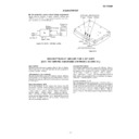
Figure 46 BLOCK DIAGRAM OF IC
IC101 VHiCS493264-1: DSP (CS493264) (3/3)
Pin No.
Function
Terminal Name
Input/Output
43
SCLK
Input
Bidirectional digital-audio output bit clock. SCLK can be an output that is derived
from MCLK to provide 32 Fs, 64 Fs, 128 Fs, 256 Fs, or 512 Fs, depending on the
from MCLK to provide 32 Fs, 64 Fs, 128 Fs, 256 Fs, or 512 Fs, depending on the
MCLK rate and the digital-output configuration. SCLK can also be an input and
must be at least 48 Fs or greater. As an input, SCLK is independent of MCLK.
44
MCLK
Input
Bidirectional master audio clock. MCLK can be an output from the CS493XX that
provides an oversampled audio-output clock at either 128 Fs, 256 Fs, or 512 Fs.
MCLK can be an input at 128 Fs, 256 Fs, 384 Fs, or 512 Fs. MCLK is used to
derive SCLK and LRCLK when SCLK and LRCLK are driven by the CS493XX.
provides an oversampled audio-output clock at either 128 Fs, 256 Fs, or 512 Fs.
MCLK can be an input at 128 Fs, 256 Fs, 384 Fs, or 512 Fs. MCLK is used to
derive SCLK and LRCLK when SCLK and LRCLK are driven by the CS493XX.
1
2
3
4
5
6
40
41
42
43
44
23
22
21
20
19
18
28
27
26
25
24
7
8
9
10
11
12
13
14
14
15
16
17
39
38
37
36
35
34
33
32
32
31
30
29
IC101
CS493264
MCLK
DGND1
CS
SCDIO, SCDOUT, PSEL, GPIO9
ABOOT, INTERQ
EXTMEM, GPIO8
SDATAN1
VD3
DGND3
SCLKN1, STCCLK2
LRCLKN1
CMPDAT, SDATAN2
CMPCLK, SCLKN2
AUDATA3, XMT958
WR, DS, EMWR, GPIO10
RD, R/W, EMOE, GPIO11
A1, SCDIN
AUDATA11
AUDATA1
AUDATA0
LRCLK
SCLK
A0, SCCLK
VD2
DGND2
DATA7, EMDA7, GPIO7
DATA6, EMDA6, GPIO6
DATA5, EMDA5, GPIO5
DATA4, EMDA4, GPIO4
DATA3, EMDA3, GPIO3
DATA2, EMDA2, GPIO2
DATA1, EMDA1, GPIO1
DATA0, EMDA0, GPIO0
CMPREQ, LRCLKN2
CLKIN
CLKSEL
FILT2
FILT1
VA
AGND
RESET
DD
DC
AUDATA2
– 47 –
SD-AT50H
1*
XTO
Output
Crystal resonator output pin.
2
XTI
Input
Crystal resonator input pin.
EXTCLK
Input
Master clock input pin.
3
TVDD
Input
Power supply pin for the output buffer. 2.7 V – 5.5 V.
4
DVSS
—
Digital ground pin. 0 V.
5
DVDD
Input
Digital power supply pin. 4.5 V – 5.5 V.
6*
TX
Output
Transmit channel (through data) output pin.
7
MCKO
Output
Master clock output pin.
8
LRCK
Input/Output
Input/output channel clock pin.
9
BICK
Input/Output
Audio serial data clock pin.
10
SDTO
Output
Audio serial data output pin.
11
SDTI1
Input
DAC1 audio serial data input pin.
12
SDTI2
Input
DAC2 audio serial data input pin.
13
SDTI3
Input
DAC3 audio serial data input pin.
14*
INT0
Output
Interrupt 0 pin.
15
INT1
Output
Interrupt 1 pin.
16
CDTO
Output
Control data output pin. (In the 4-line serial mode)
CAD1
Input
Chip address 1 pin. (In the I
2
C bus mode)
17
CDTI
Input
Control data input pin. (In the 4-line serial mode)
SDA
Input/Output
Control data input/output pin. (In the I
2
C bus mode)
18
CCLK
Input
Control data clock pin. (In the 4-line serial mode)
SCL
Input
Control data clock pin. (In the I
2
C bus mode)
19
CSN
Input
Chip select pin. (In the 4-line serial mode)
CAD0
Input
Chip address 0 pin. (In the I
2
C bus mode)
20
DZF2
Output
Zero input detect 2 pin. (Note 1)
When the input data of group 2 is “0” for 8192 times in a row or the RSTN bit is “0”, it
changes to “H”.
changes to “H”.
OVF
Output
Analog input overflow detect pin. (Note 2)
It changes to “H” if the analog input of Lch or Rch overflows.
21
AVSS
—
Analog ground pin. 0 V.
22
AVDD
Input
Analog power supply pin. 4.5 V – 5.5 V.
23
VREFH
Input
Reference voltage input pin. AVDD.
24
VCOM
Output
Common voltage output pin. AVDD/2.
25*
DZF1
Output
Zero input detect 1 pin. (Note 1)
When the input data of group 1 is “0” for 8192 times in a row or the RSTN bit is “0”, it
changes to “H”.
changes to “H”.
26
LOUT3
Output
DAC3 L channel analog output pin.
27
ROUT3
Output
DAC3 R channel analog output pin.
28
LOUT2
Output
DAC2 L channel analog output pin.
29
ROUT2
Output
DAC2 R channel analog output pin.
30
LOUT1
Output
DAC1 L channel analog output pin.
31
ROUT1
Output
DAC1 R channel analog output pin.
32
LIN
Input
L channel analog input pin.
33
RIN
Input
R channel analog input pin.
34
PVDD
Input
PLL power supply pin. 4.5 V – 5.5 V.
35
R
—
External resistor pin.
36
PVSS
—
PLL ground pin. 0 V.
37*
RX4
Input
Receiver channel input 4 pin. (Internal bias pin)
38
SLAVE
Input
Slave mode pin. “L” : master mode or slave mode, “H” : slave mode
39*
RX3
Input
Receiver channel input 3 pin. (Internal bias pin)
40
TST
Input
Test pin. Connect to DVSS.
IC102 VHiAK4586VQ-1: ADC/DAC/DIR Converter (AK4586VQ) (1/2)
Terminal Name
Pin No.
Input/Output
Function
In this unit, the terminal with asterisk mark (*) is (open) terminal which is not connected to the outside.

