Read Sharp CD-CH1500 (serv.man8) Service Manual online
– 49 –
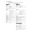
CD-CH1500H/CD-CH1500W
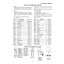
SW756
PLAY/PAUSE
ON—OFF
SW757
STOP
ON—OFF
SW758
PLAY
ON—OFF
SW761
AUX
ON—OFF
SW762
TUNER
ON—OFF
SW763
TAPE
ON—OFF
SW764
CD
ON—OFF
SW772
EQUALIZER MODE
ON—OFF
SW773
X-BASS
ON—OFF
SW778
ENTER
ON—OFF
SW783
PLAY MODE
ON—OFF
SW784
DISPLAY
ON—OFF
SW786
MENU
ON—OFF
SW901
SPAN SELECTOR
9 kHz/50 kHz—
(CD-CH1500W ONLY)
10 kHz/100 kHz
SWB101
DISC DETECT 1
ON—OFF
SWB102
DISC DETECT 2
ON—OFF
SWB103
DISC DETECT 3
ON—OFF
SWB104
MODE 1
ON—OFF
SWB105
MODE 2
ON—OFF
SWB106
MODE 3
ON—OFF
SWB107
MODE 4
ON—OFF
SWB108
MODE 5
ON—OFF
SWB109
TRAY 1
ON—OFF
SWB110
TRAY 2
ON—OFF
•
Schematic diagram and Wiring Side of P.W.Board for this
model are subject to change for improvement without prior
notice.
notice.
•
The indicated voltage in each section is the one measured
by Digital Multimeter between such a section and the chas-
sis with no signal given.
1. In the tuner section,
sis with no signal given.
1. In the tuner section,
indicates FM stereo
2. In the power section, a tape is being played back.
3. In the CD section, the CD is stopped.
3. In the CD section, the CD is stopped.
•
Parts marked with “
1
” ( ) are important for
maintaining the safety of the set. Be sure to replace these
parts with specified ones for maintaining the safety and
performance of the set.
parts with specified ones for maintaining the safety and
performance of the set.
NOTES ON SCHEMATIC DIAGRAM
•
Resistor:
To differentiate the units of resistors, such symbol as K and
M are used: the symbol K means 1000 ohm and the symbol
M means 1000 kohm and the resistor without any symbol is
ohm-type resistor. Besides, the one with “Fusible” is a fuse
type.
M are used: the symbol K means 1000 ohm and the symbol
M means 1000 kohm and the resistor without any symbol is
ohm-type resistor. Besides, the one with “Fusible” is a fuse
type.
•
Capacitor:
To indicate the unit of capacitor, a symbol P is used: this
symbol P means pico-farad and the unit of the capacitor
without such a symbol is microfarad. As to electrolytic
capacitor, the expression “capacitance/withstand voltage”
is used.
(CH), (TH), (RH), (UJ): Temperature compensation
(ML): Mylar type
(P.P.): Polypropylene type
symbol P means pico-farad and the unit of the capacitor
without such a symbol is microfarad. As to electrolytic
capacitor, the expression “capacitance/withstand voltage”
is used.
(CH), (TH), (RH), (UJ): Temperature compensation
(ML): Mylar type
(P.P.): Polypropylene type
SO801
VOLTAGE SELECTOR
110 V—127 V—
(CD-CH1500W ONLY)
220 V—230-240 V
NSW1
PICKUP IN
ON—OFF
SW701
ON/STAND-BY
ON—OFF
SW705
OPEN/CLOSE
ON—OFF
SW710
PANEL OPEN/CLOSE
ON—OFF
SW711
VOLUME DOWN
ON—OFF
SW712
VOLUME UP
ON—OFF
SW720
CD 1 EJECT
ON—OFF
SW721
CD 2 EJECT
ON—OFF
SW722
CD 3 EJECT
ON—OFF
SW723
CD 4 EJECT
ON—OFF
SW724
CD 5 EJECT
ON—OFF
SW725
CD 6 EJECT
ON—OFF
SW730
CD 1 PLAY
ON—OFF
SW731
CD 2 PLAY
ON—OFF
SW732
CD 3 PLAY
ON—OFF
SW733
CD 4 PLAY
ON—OFF
SW734
CD 5 PLAY
ON—OFF
SW735
CD 6 PLAY
ON—OFF
SW750
REVERSE MODE
ON—OFF
SW751
CLEAR
ON—OFF
SW752
MEMORY
ON—OFF
SW753
FAST REVERSE
ON—OFF
SW754
FAST FORWARD
ON—OFF
SW755
TAPE RECORD
ON—OFF
REF. NO
DESCRIPTION
POSITION
POSITION
REF. NO
DESCRIPTION
TYPES OF TRANSISTOR AND LED
E C B
(S) (G) (D)
FRONT
VIEW
FRONT
VIEW
VIEW
B C E
FRONT
VIEW
2SA562 Y
2SA1015 GR
2SB561 C
2SB562 C
2SB1565 F
2SC380 O
2SC1740 R
DTC363 TS
KRA102 M
KRA107 M
KRC102 M
2SA1015 GR
2SB561 C
2SB562 C
2SB1565 F
2SC380 O
2SC1740 R
DTC363 TS
KRA102 M
KRA107 M
KRC102 M
2SD2012
HLMP1700
K5052UL
LNG995PF
L934MBC5
K5052UL
LNG995PF
L934MBC5
SVC211C
SVC348S
SVC348S
1 2 3
(1) (2) (3)
KRC104 M
KRC107 M
KTA1046 Y
KTA1266 GR
KTA1271 Y
KTC2026
KTC3194 Y
KTC3199 GR
KTC3203 Y
KRC107 M
KTA1046 Y
KTA1266 GR
KTA1271 Y
KTC2026
KTC3194 Y
KTC3199 GR
KTC3203 Y
CD-CH1500H/CD-CH1500W
– 50 –
FUNCTION TABLE OF IC
IC2 VHiTC9490F/-1: Servo/Signal Control (TC9490F) (1/2)
1*
BCK
Output
Bit clock output terminal. 32 fs, 48 fs or 64 fs can be selected by command.
2*
LRCK
Output
L/R channel clock output terminal. L channel: "L", R channel: "H".
the output polarity can be inverted by command.
the output polarity can be inverted by command.
3*
AOUT
Output
Audio data output terminal. MSB/LSB fast can be selected by command.
4
DOUT
Output
Digital out output terminal. Up to double speed can be output.
5*
IPF
Output
Correction flag output terminal. When the correction impossible symbol appears if the AOUT
output corresponds to the C2 correction output: "H".
output corresponds to the C2 correction output: "H".
6
DVDD
Input
Digital 3.3 V power supply terminal.
7
DVSS
—
Digital GND terminal.
8*
SBOK
Output
Subcode Q data CRCC decision result output terminal. When the decision result is OK: "H".
9*
CLCK
Input/Output
Clock input/output terminal for subcodes P-W data reading.
The input/output polarity can be selected by command.
The input/output polarity can be selected by command.
10*
DATA
Output
Subcodes P-W data output terminal.
11*
SFSY
Output
Playback system frame sync signal output terminal.
12*
SBSY
Output
Subcode block sync output terminal.
In the S1 position when the subcode sync is detected: "H".
In the S1 position when the subcode sync is detected: "H".
13,14*
/HSO,/UHSO
Output
Playback speed mode flag output terminal.
15
PVDD
Input
3.3 V power supply terminal for PLL system.
16
PDO
Output
EFM signal/PLCK signal phase error signal output terminal.
17
TMAX
Output
TMAX detection result output terminal.
18
LPFN
Input
Amp's inversion input terminal for PLL system low-pass filter.
19
LPFO
Output
Amp's output terminal for PLL system low-pass filter.
20
PVREF
—
VREF terminal only for PLL system.
21
VCOF
Output
Filter terminal for VCO.
22
AVSS
—
Analog GND terminal.
23
SLCO
Output
DAC output terminal for data slice level generation.
24
RFI
Input
RF signal input terminal. Zin can be selected by command.
25
AVDD
Input
Analog 3.3 V power supply terminal.
26
RFCT
Input
RFRP signal center level input terminal.
27
RFZI
Input
Input terminal for RFRP signal zero crossing.
28
RFRP
Input
RF ripple signal terminal.
29
FEI
Input
Focus error signal input terminal.
30
SBAD
Input
Sub-beam addition signal input terminal.
31
TEI
Input
Tracking error input terminal. Fetch when the tracking servo is on.
32
TEZI
Input
Input terminal for tracking error signal zero crossing.
33
FOO
Output
Focus equalizer output terminal.
34
TRO
Output
Tracking equalizer output terminal.
35
VREF
Input
Analog reference power supply terminal.
36
RFGC
Output
RF amplitude adjustment control signal output terminal.
37
TEBC
Output
Tracking balance control signal output terminal.
38
SEL
Output
APC circuit ON/OFF signal output terminal.
When the laser is on, UHS= "L": "Hi-z", UHS= "H": "H" output.
When the laser is on, UHS= "L": "Hi-z", UHS= "H": "H" output.
Pin No.
Terminal Name
Function
Input/Output
In this unit, the terminal with asterisk mark (*) is (open) terminal which is not connected to the outside.
H
H
Normal speed playback
H
L
Double speed playback
L
L
4-time speed playback
—
—
—
/UHSO
/HSO
Playback speed
Longer than the specified period
"PVDD3"
Within the specified period
"Hi-z"
Shorter than the specified period
"AVSS3"
TMAX detection result
TMAX output
– 51 –
CD-CH1500H/CD-CH1500W
IC2 VHiTC9490F/-1: Servo/Signal Control (TC9490F) (2/2)
39
AVDD3
Input
Analog 3.3 V power supply terminal.
40
FMO
Output
Feed equalizer output terminal.
41
DMO
Output
Disc equalizer output terminal.
42
DVSS
—
Digital GND terminal.
43
DVDD
Input
Digital 3.3 V power supply terminal.
44
TESIN
Input
Test input terminal. Usually "L" fixed.
45
XVSS
—
GND terminal for system clock oscillation circuit.
46
XI
Input
System clock oscillation circuit input terminal.
47
XO
Output
System clock oscillation circuit output terminal.
48
XVDD
Input
3.3 V power supply terminal for system clock oscillation circuit.
49
DVSS
—
GND terminal for D/A converter.
50
RO
Output
R channel data normal rotation output terminal.
51
DVDD
Input
3.3 V power supply terminal for D/A converter.
52
DVR
—
Reference voltage terminal.
53
LO
Output
L channel data normal rotation output terminal.
54
DVSS
—
D/A converter section GND terminal.
55*
ZDET
Output
1-bit D/A converter 0 detection flag output terminal.
56
VSS
—
GND terminal for microcomputer interface.
57-60
BUS0-BUS3
Input/Output
Data input/output terminal for microcomputer interface.
61
BUCK
Input
Clock input terminal for microcomputer interface.
62
/CCE
Input
Chip enable signal input terminal for microcomputer interface.
In case of "L", BUS3-0 are active.
In case of "L", BUS3-0 are active.
63
/RST
Input
Reset signal input terminal. Reset: "L".
64
VDD
Input
5 V power supply terminal for microcomputer interface.
Pin No.
Terminal Name
Function
Input/Output
In this unit, the terminal with asterisk mark (*) is (open) terminal which is not connected to the outside.
Note:
AI/F: Analog input/output terminal
3-5I/F: Terminal with a built-in 3-5 interface (5 V system input/output terminal)
3I/F: 3 V system input/output terminal
Note:
AI/F: Analog input/output terminal
3-5I/F: Terminal with a built-in 3-5 interface (5 V system input/output terminal)
3I/F: 3 V system input/output terminal
Figure 51 BLOCK DIAGRAM OF IC
XVDD
XO
XI
XVSS
TESIN
DVDD
DVSS
DMO
FMO
AVDD3
SEL
TEBC
RFGC
VREF
TRO
FOO
TEZI
TEI
SBAD
FEI
RFRP
RFZI
RFCT
AVDD
RFI
SLCO
AVSS
VCOF
PVREF
LPFO
LPFN
TMAX
PDD
PVDD
/HSO
/UHSO
SBSY
SFSY
DATA
CLCK
SBOK
DVSS
DVDD
IPF
DOUT
AOUT
LRCK
BCK
DVSS
RO
DVDD
DVR
LO
DVSS
ZDET
VSS
BUS1
BUS2
BUS3
BUCK
/CCE
/RST
VDD
1
2
3
4
5
6
7
8
9
10
11
12
13
14
15
16
17
18
19
20
21
22
23
24
25
26
27
28
29
30
31
32
33
34
35
36
37
38
39
40
41
42
43
44
45
46
47
48
49
50
51
52
53
54
55
56
57
58
59
60
61
62
63
64
LPF
1-bit
DAC
PWM
D/A
A/D
VCO
ROM
RAM
16K RAM
PLL
TMAX
+
+
+
+
BUS0
Clock
generator
Servo control
Digital equalizer
adjustment circuit
Data
slicer
CLV
servo
Synchronizing
signal guarantee
EFM demodulation
Sub-code
demodulation
circuit
Address
circuit
Correction
circuit
Digital
out
Audio output
circuit
Microcomputer
interface
CD-CH1500H/CD-CH1500W
– 52 –
IC6 VHiTA2147F/-1: Servo Pre Amp. (TA2147F)
1
VCC
Input
3.3 V power supply terminal.
2
FNI
Input
Main beam amp input terminal.
3
FPI
Input
Main beam amp input terminal
4
TPI
Input
Sub-beam amp input terminal.
5
TNI
Input
Sub-beam amp input terminal.
6
MDI
Input
Monitor photodiode amplifier input terminal.
7
LDO
Output
Laser diode amp output terminal.
8
SEL
Input
APC circuit ON/OFF signal, LDO terminal control input terminal and bottom/peak
detection frequency switching terminal.
detection frequency switching terminal.
9
TEB
Input
Tracking error balance adjustment signal input terminal.
• TEBC input voltage.
• TEBC input voltage.
10
TEN
Input
Tracking error signal generation amp antiphase input terminal.
11
TEO
Output
Tracking error signal generation amp output terminal.
12
SBAD
Output
RF signal peak detection output terminal.
13
GVSW
Input
AGC, FE, TE amp gain switching terminal.
14
VRO
Output
Reference voltage (VRO) output terminal. • VCC= 3.3 V: VRO= 1/2 VCC
15
FEO
Output
Focus error signal generation amp output terminal.
16
FEN
Input
Focus error signal generation amp antiphase input terminal.
17
RFRP
Output
Signal generation amp output terminal for track count.
18
RFIS
Input
Signal generation amp input terminal for track count.
19
RFGO
Output
RF signal amplitude adjustment amp output terminal.
20
RFGC
Input
RF amplitude adjustment control signal input terminal. • RFGC input voltage.
21
AGCI
Input
RF signal amplitude adjustment amp input terminal.
22
RFO
Output
RF signal generation amp output terminal.
23
RFN
Input
RF signal generation amp input terminal.
24
GND
—
GND terminal.
Terminal Name
Pin No.
Input/Output
Function
GND
OFF
Connection to VCC via 1 k
Ω
Hi-z
ON
Control signal output
VCC
ON
Control signal output
SEL
APC circuit
LDO
GND
CD-RW
Hi-z
CD-DA
VCC
CD-CA
GVSW
Mode
Figure 52 BLOCK DIAGRAM OF IC
PIN
SEL
(APC_SW)
TEB
(TE_BAL)
RFGC
(AGC_Gain)
GVSW
(CD/RW)
V
CTRL
V
CC
HiZ
GND
APC ON
APC ON
APC OFF
(LDO=H)
-50%
0%
+50%
+12dB
+6dB
0dB
DA
(0dB)
DA
(0dB)
RW
(+12dB)
GVSW
VRO
FEO
FEN
RFRP
20K
20K
20K
15K
15K
10p
50u
20
µ
12K
20K
20K
20K
2K
40K
50K
50K
40K
10p
1.3V
1K
14K
2K
SBAD
TEO
TEN
TEB
SEL
LDO
MDI
TNI
TPI
FPI
FNI
VCC
80K
80K
20K
20K
240K
15p
240K
15p
180K
40p
40p
60k
60k
180K
40K
20K
30K
3K
20K
12K
RFGC
AGCI
RFO
RFN
GND
RFIS
RFGO
3K
1
2
3
4
5
6
7
8
9
10
11
12
13
14
15
16
17
18
19
20
21
22
23
24
BOTTOM
PEAK
PEAK
K
x0.5
x2
x2
x0.5
1

