Read Sharp CD-BA3000 (serv.man6) Service Manual online
CD-BA3000H
– 36 –
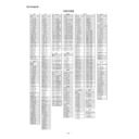
0V
0V
0V
0V
0V
0V
4.6V
4.6V
0V
2.6V
4.9V
4.7V
4.9V
4.6V
0V
0V
4.6V
4.6V
4.6V
0V
0V
0V
4.8V
0V
4.9V
4.8V
0V
0V
0V
0V
0V
4.9V
5.0V
4.9V
4.6V
5.0V
4.9V
4.9V
0V
4.8V
9
8
7
6
5
4
3
2
1
30
29
28
27
26
25
24
23
22
21
20
19
18
17
16
15
14
13
12
11
10
40
39
38
37
36
35
34
33
32
31
PIN
NO.
NO.
VOLTAGE
IC701
PIN VOLTAGE
4.9V
4.9V
0V
0V
4.9V
–29.8V
–27.5V
–29.7V
–18.5V
–29.7V
–29.7V
4.9V
4.9V
0V
34.3V
–20.1V
–16.4V
–12.2V
–16.5V
–14.2V
–31.9V
–31.9V
–18.8V
–18.8V
60
59
58
57
56
55
54
53
52
51
61
74
73
72
71
70
69
68
67
66
65
64
63
62
–31.8V
–31.8V
–31.9V
–20.5V
–20.6V
–27.6V
–27.7V
–23.4V
–23.1V
–20.9V
–34.1V
–18.9V
–28.7V
–26.0V
–29.8V
–29.7V
78
77
76
75
79
90
89
88
87
86
85
84
83
82
81
3.0V
1.9V
9.1V
9.1V
0V
3.8V
4.6V
4.5V
4.5V
4.9V
50
49
48
47
46
45
44
43
42
41
–31.9V
–31.9V
–31.9V
–31.9V
–31.9V
–31.9V
–32.0V
–31.9V
–31.9V
–31.9V
100
99
98
97
96
95
94
93
92
91
80
1.9V
4.9V
0V
0V
1.6V
1.6V
2.1V
0V
0V
0V
0V
0V
2.1V
2.1V
2.1V
1.6V
1.6V
1.8V
2.1V
0V
0V
2.1V
4.9V
3.5V
4.9V
1.6V
2.1V
2.1V
0V
0V
0V
0V
0V
0V
0V
4.2V
9
8
7
6
5
4
3
2
1
30
29
28
27
26
25
24
23
22
21
20
19
18
17
16
15
14
13
12
11
10
36
35
34
33
32
31
0V
2.1V
2.1V
4.9V
2.1V
41
2.1V
42
40
39
38
37
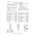
PIN
NO. VOLTAGE
IC3
9V
9V
0V
0V
0V
0V
9V
5V
9V
0V
9V
0V
9
8
7
6
5
4
3
2
1
12
11
10
9V
5V
1.8V
9V
0V
5V
17
16
15
14
13
18
PIN
NO.
VOLTAGE
IC702
–37V
37V
77.6V
0V
37V
37V
–23V
–77V
0V
0V
0V
0V
9
8
7
6
5
4
3
2
1
12
11
10
0V
3.1V
0V
15
14
13
–75V
75V
0V
18
17
16
0V
0V
–75V
21
20
0V
0V
23
22
19
PIN
NO.
VOLTAGE
IC901
4.6V (4.9V)
0V (0V)
2.1V (2.1V)
4.5V (4.8V)
2.1V (2.1V)
2.1V (2.1V)
4.6V (4.9V)
2.4V (3.2V)
4.5V (4.8V)
3.9V (0V)
3.3V (1.8V)
3.3V (1.1V)
9
8
7
6
5
4
3
2
1
12
11
10
1.2V (1.2V)
3.5V (2.0V)
1.2V (1.2V)
2.0V (2.0V)
2.7V (0V)
2.1V (0.9V)
0V (1.9V)
0.3V (0.9V)
17
16
15
14
13
20
19
18
2.6V (2.0V)
2.6V (2.0V)
4.5V (4.8V)
3.0V (3.3V)
21
24
23
22
PIN
NO.
VOLTAGE
IC303
2.8V (0.2V)
0V (0V)
0.8V (0V)
1.5V (0V)
3.6V (0.4V)
1.5V (0V)
3.6V (0.4V)
3.5V (0.3V)
3.6V (0.3V)
9
8
7
6
5
4
3
2
1
PIN
NO.
VOLTAGE
IC301
13.0V
12.8V
13.0V
13.0V
12.8V
0V
13.0V
18.3V
8
7
6
5
4
3
2
1
PIN
NO.
VOLTAGE
IC562
13.1V
1.3V
13.1V
13.1V
1.3V
0V
13.1V
18.3V
8
7
6
5
4
3
2
1
PIN
NO.
VOLTAGE
IC561
13.1V
1.4V
13.1V
13.1V
1.4V
0V
13.1V
18.3V
8
7
6
5
4
3
2
1
PIN
NO.
VOLTAGE
IC563
0V
0V
–6V
2V
0.6V
–7.6V
0V
6.3V
8
7
6
5
4
3
2
1
PIN
NO.
VOLTAGE
IC860
20V
0V
5.0V
3
2
1
PIN
NO.
VOLTAGE
Q852
20V
0V
10V
3
2
1
PIN
NO.
VOLTAGE
Q851
10V
20V
9.5V
3
2
1
PIN
NO.
VOLTAGE
Q850
0V
3.0V
3.3V
3.3V
0V
0V
0V
1.6V
1.6V
1.6V
1.6V
1.6V
1.6V
1.6V
1.7V
4.7V
0V
1.6V
0V
2.4V
3.3V
0V
1.6V
3.0V
0V
3.3V
0V
0.7V
0V
0V
0V
0V
0V
1.6V
3.3V
0V
1.6V
1.6V
1.6V
1.6V
0V
2.1V
2.1V
0V
3.3V
3.5V
3.3V
3.3V
3.3V
1.6V
1.6V
1.5V
0V
1.5V
3.0V
3.3V
1.8V
3.0V
0V
0V
0V
1.7V
2.4V
0V
9
8
7
6
5
4
3
2
1
30
29
28
27
26
25
24
23
22
21
20
19
18
17
16
15
14
13
12
11
10
50
49
48
47
46
45
44
43
42
41
40
39
38
37
36
35
34
33
32
31
PIN
NO. VOLTAGE
51
64
63
62
61
60
59
58
57
56
55
54
53
52
3.4V
0V
0V
3.2V
0V
0V
0V
0V
0V
4.8V
4.9V
4.9V
4.6V
0V
4.9V
0V
68
67
66
65
69
80
79
78
77
76
75
74
73
72
71
70
IC2
0V (0V)
0V (0V)
0V (0V)
0V (0V)
0.5V (0.5V)
1.9V (1.9V)
0V (0V)
0.6V (0.6V)
3.3V (3.3V)
3.3V (3.3V)
0V (0V)
0V (0V)
9
8
7
6
5
4
3
2
1
12
11
10
0V (0V)
6.7V (6.7V)
4.0V (4.0V)
3.3V (3.3V)
0.6V (0.6V)
0V (0V)
0V (0V)
0V (0V)
17
16
15
14
13
20
19
18
1.9V (1.9V)
0.5V (0.5V)
0V (0V)
0V (0V)
21
24
23
22
PIN
NO.
VOLTAGE
IC101
0.1V (9.9V)
2.9V (2.9V)
2.4V (2.4V)
0V (0V)
0V (0V)
0V (0V)
4.8V (4.9V)
4.2V (0V)
3.3V (0V)
0V (3.9V)
5.1V (5.1V)
2.2V (0V)
9
8
7
6
5
4
3
2
1
12
11
10
0V (2.4V)
5.0V (5.0V)
0V (0V)
2.3V (0V)
5.0V (5.0V)
0.6V (0.8V)
0.8V (1.8V)
2.0V (1.0 V)
17
16
15
14
13
20
19
18
0V (0V)
2.5V (3.0V)
21
22
22
PIN
NO.
VOLTAGE
IC302
1.6V
0V
1.6V
1.6V
1.6V
0V
0V
1.6V
3.3V
0V
0V
0V
0V
1.6V
1.6V
1.6V
1.6V
1.6V
1.6V
2.6V
1.6V
1.6V
1.6V
1.6V
1.6V
0V
0V
0V
1.6V
3.3V
9
8
7
6
5
4
3
2
1
30
29
28
27
26
25
24
23
22
21
20
19
18
17
16
15
14
13
12
11
10
PIN
NO. VOLTAGE
IC1
5.0V
0V
5.0V
3
2
1
PIN
NO.
VOLTAGE
IC704
0V
2.72V
2.6V
2.59V
5.2V
0V
2.55V
0V
0V
0V
0V
2.66V
9
8
7
6
5
4
3
2
1
12
11
10
0V
2.56V
5.21V
0V
0V
1.4V
1.7V
4.6V
17
16
15
14
13
20
19
18
4.3V
0V
21
22
22
PIN
NO.
VOLTAGE
ICT21
0V
0V
23
24
24
VOLTAGE
– 37 –
CD-BA3000H
T
T
EFBL
FDO
TE
Stopped
CH1=500mV
DC 10:1
CH2=200mV
DC 10:1
CH3=1V
DC 10:1
500ms/div
(500ms/div)
NORM:20kS/s
1
2
3
=Record Length=
Smoothing : ON
CH1 : 0.000V
CH2 : 0.000V
CH2 : 0.000V
Main : 100K
Zoom : 2k
Zoom : 2k
Mode : SINGLE
Type : EDGE CH1
Delay : 0.0ns
Hold off : 0.2
Type : EDGE CH1
Delay : 0.0ns
Hold off : 0.2
µ
s
CH3 : 0.00V
CH4 : 0.00V
CH4 : 0.00V
BW : FULL
=Trigger=
=Filter=
=Offset=
CH2
v/DIV
200mV
v/DIV
200mV
1999/04/05 20:26:47
1
IC2 24
4
IC1 18 ,
IC2 16
IC1 13 ,
IC2 22
13
T
T
DATA
DATACK
LRSY
Stopped
CH1=2V
DC 10:1
CH2=2V
DC 10:1
CH3=2V
DC 10:1
5us/div
(5us/div)
NORM:100kS/s
1
2
3
=Record Length=
Smoothing : ON
CH1 : 0.00V
CH2 : 0.00V
CH2 : 0.00V
Main : 5K
Zoom : 100
Zoom : 100
Mode : AUTO
Type : EDGE CH3
Delay : 0.0ns
Hold off : 0.2
Type : EDGE CH3
Delay : 0.0ns
Hold off : 0.2
µ
s
CH3 : 0.00V
CH4 : 0.00V
CH4 : 0.00V
BW : FULL
=Trigger=
=Filter=
=Offset=
CH3
v/DIV
2 V
v/DIV
2 V
1999/04/05 20:50:17
10
IC2 57
IC2 58
IC2 59
11
12
T
T
DOUT
Stopped
CH1=2V
DC 10:1
500ns/div
1999/04/07 09:25:28
(500ns/div)
NORM:200MS/s
1
=Record Length=
Smoothing : ON
CH1 : 0.00V
CH2 : 0.00V
CH2 : 0.00V
Main : 1K
Zoom : 100
Zoom : 100
Mode : NORMAL
Type : EDGE CH1
Delay : 2.887ms
Hold off : 0.2
Type : EDGE CH1
Delay : 2.887ms
Hold off : 0.2
µ
s
CH3 : 0.00V
CH4 : 0.00V
CH4 : 0.00V
BW : FULL
=Trigger=
=Filter=
=Offset=
9
IC2 37
T
FDO
PDO2
PDO1
Stopped
CH1=500mV
DC 10:1
CH3=1V
DC 10:1
CH4=1V
DC 10:1
500ms/div
(500ms/div)
NORM:20kS/s
1
4
3
=Record Length=
Smoothing : ON
CH1 : 0.000V
CH2 : 0.0V
CH2 : 0.0V
Main : 100K
Zoom : 2K
Zoom : 2K
Mode : AUTO
Type : EDGE CH2
Delay : 0.0ns
Hold off : 0.2
Type : EDGE CH2
Delay : 0.0ns
Hold off : 0.2
µ
s
CH3 : 0.00V
CH4 : 0.00V
CH4 : 0.00V
BW : FULL
=Trigger=
=Filter=
=Offset=
CH1
v/DIV
500mV
v/DIV
500mV
1999/04/05 17:33:17
1
IC2 24
7
IC2 1
8
IC2 2
T
T
FDO
SPDO
Stopped
CH1=200mV
DC 10:1
CH2=500mV
DC 10:1
500ms/div
1999/04/07 09:51:15
(500ms/div)
NORM:20kS/s
2
1
=Record Length=
Smoothing : ON
CH1 : 0.000V
CH2 : 0.000V
CH2 : 0.000V
Main : 100K
Zoom : 2K
Zoom : 2K
Mode : NORMAL
Type : EDGE CH2
Delay : 2.924ms
Hold off : 0.2
Type : EDGE CH2
Delay : 2.924ms
Hold off : 0.2
µ
s
CH3 : 0.00V
CH4 : 0.00V
CH4 : 0.00V
BW : FULL
=Trigger=
=Filter=
=Offset=
1
IC2 24
6
IC2 25
T
T
TE
DRF
Stopped
CH1=10V
DC 10:1
CH2=1V
DC 10:1
100ms/div
(100ms/div)
NORM:100kS/s
2
1
=Record Length=
Smoothing : ON
CH1 : 0.0V
CH2 : 0.00V
CH2 : 0.00V
Main : 100K
Zoom : 2K
Zoom : 2K
Mode : NORMAL
Type : EDGE CH1
Delay : 2.924ms
Hold off : 0.2
Type : EDGE CH1
Delay : 2.924ms
Hold off : 0.2
µ
s
CH3 : 0.00V
CH4 : 0.00V
CH4 : 0.00V
BW : FULL
=Trigger=
=Filter=
=Offset=
3
IC2 72
4
IC1 18 ,
IC2 16
Vp-p=1.0V~1.3V
0.5mV/div,0.5
µ
sec/div
5
IC1 27
T
FDO
DRF
TE
Stopped
CH1=500mV
DC 10:1
CH2=10V
DC 10:1
CH3=1V
DC 10:1
500ms/div
(500ms/div)
NORM:20kS/s
1
2
3
=Record Length=
Smoothing : ON
CH1 : 0.000V
CH2 : 0.0V
CH2 : 0.0V
Main : 100K
Zoom : 2K
Zoom : 2K
Mode : AUTO
Type : EDGE CH1
Delay : 0.0ns
Hold off : 0.2
Type : EDGE CH1
Delay : 0.0ns
Hold off : 0.2
µ
s
CH3 : 0.00V
CH4 : 0.00V
CH4 : 0.00V
BW : FULL
=Trigger=
=Filter=
=Offset=
-3div
-1div
0div
+1div
+3div
CH Position To
CH2
Position
0.20div
Position
0.20div
1
IC2 24
3
IC2 72
4
IC1 18 ,
IC2 16
T
FDO
TDO
Stopped
CH1=500mV
DC 10:1
CH3=500mV
DC 10:1
500ms/div
(500ms/div)
NORM:20kS/s
1
3
=Record Length=
Smoothing : ON
CH1 : 0.000V
CH2 : 0.0V
CH2 : 0.0V
Main : 100K
Zoom : 2K
Zoom : 2K
Mode : AUTO
Type : EDGE CH1
Delay : 0.0ns
Hold off : 0.2
Type : EDGE CH1
Delay : 0.0ns
Hold off : 0.2
µ
s
CH3 : 0.000V
CH4 : 0.00V
CH4 : 0.00V
BW : FULL
=Trigger=
=Filter=
=Offset=
CH1
v/DIV
500mV
v/DIV
500mV
1
IC2 24
2
IC2 23
WAVEFORMS OF CD CIRCUIT
CD-BA3000H
– 38 –
HOW TO USE
CAUTION
Cleaning fluid
Cleaner disc
Using the brush in the cleaner cap, apply 1 or 2 drops of the cleaning fluid to the
brush on the CD cleaner disc which has the mark next to it.
Place the CD cleaner disc onto the CD disc tray with the brush side down,then
press the play button.
You will hear music for about 20 seconds and the CD player will automatically stop.
If it continuous to turn, press the stop button.
1.
2.
3.
The CD lens cleaner should be effective for 30-50 operations, however if the
brushes become worn out earlier then please the cleaner disc.
If the CD cleaner brushes become very wet then wipe off any excess fluid with a soft
cloth.
Do not drink the cleaner fluid or allow it to come in contact with the eyes. In the
event of this happening then drink and / or rinse with clean water and seek medical
advice.
The CD cleaner disk must not be used on car CD players or on computer CD-ROM
drives.
All rights reserved.Unauthorized duplicating, broadcasting and renting this product is
prohibited by law.
Parts code
1.
CD optical pickup Lens cleaner disc
UDSKA0004AFZZ
TROUBLE SHOOTING
When the CD does not function
When the CD section does not operate when the objective lens of the optical pickup is dirty, this section may not operate. Clean
the objective lens, and check the playback operation. When this section does not operate even after the above step is taken, check
the following items.
Remove the cabinet and follow the trouble shooting instructions.
"Track skipping and/or no TOC (Table Of Contents) may be caused by build up of dust other foreign matter on the laser pickup
lens. Before attempting any adjustment make certain that the lens is clean. If not, clean it as mentioned below."
Turn the power off.
Gently clean the lens with a lens cleaning tissue and a small amount of isopropyl alcohol.
Do not touch the lens with the bare hand.
Gently clean the lens with a lens cleaning tissue and a small amount of isopropyl alcohol.
Do not touch the lens with the bare hand.
When a CD cannot be played
1. "E-CD01" is displayed.
(1) Check the power to IC2 (LC78641E), the presence of the clock signal (16.934 MHz) and the status of the RESET terminal
(pin 71 on IC2).
(2) Does the pickup move to the PICKUP-IN Switch (SW4) position?
(pin 71 on IC2).
(2) Does the pickup move to the PICKUP-IN Switch (SW4) position?
If (1) and (2) are OK, check the system microcomputer (especially the communication line with the DSP).
2. Pressing the CD operation key is accepted, but playback does not occur.
(1) Focus-HF system check
(2) Tracking system check
(3) Spin system check
(4) PLL system check
(5) Others
(2) Tracking system check
(3) Spin system check
(4) PLL system check
(5) Others
– 39 –
CD-BA3000H
Vp-p=1.0V~1.3V
0.5mV/div,0.5
µ
sec/div
5
IC1 27
T
FDO
DRF
TE
Stopped
CH1=500mV
DC 10:1
CH2=10V
DC 10:1
DC 10:1
CH3=1V
DC 10:1
500ms/div
(500ms/div)
NORM:20kS/s
1
2
3
=Record Length=
Smoothing : ON
CH1 : 0.000V
CH2 : 0.0V
CH2 : 0.0V
Main : 100K
Zoom : 2K
Zoom : 2K
Mode : AUTO
Type : EDGE CH1
Delay : 0.0ns
Hold off : 0.2
Type : EDGE CH1
Delay : 0.0ns
Hold off : 0.2
µ
s
CH3 : 0.00V
CH4 : 0.00V
CH4 : 0.00V
BW : FULL
=Trigger=
=Filter=
=Offset=
-3div
-1div
0div
+1div
+3div
CH Position To
CH2
Position
0.20div
Position
0.20div
1
IC2 24
3
IC2 72
4
IC1 18 ,
IC2 16
T
FDO
TDO
Stopped
CH1=500mV
DC 10:1
CH3=500mV
DC 10:1
500ms/div
(500ms/div)
NORM:20kS/s
1
3
=Record Length=
Smoothing : ON
CH1 : 0.000V
CH2 : 0.0V
CH2 : 0.0V
Main : 100K
Zoom : 2K
Zoom : 2K
Mode : AUTO
Type : EDGE CH1
Delay : 0.0ns
Hold off : 0.2
Type : EDGE CH1
Delay : 0.0ns
Hold off : 0.2
µ
s
CH3 : 0.000V
CH4 : 0.00V
CH4 : 0.00V
BW : FULL
=Trigger=
=Filter=
=Offset=
CH1
v/DIV
500mV
v/DIV
500mV
1
IC2 24
2
IC2 23
If the level is not normal, check around pins 27~29 on IC1.
1. Is focus servo activated? (Waveform drawing Figure 39-2)
Pins 1~11 on IC1
Check the laser diode driver Q3 peripheral circuit.
Focus error circuit (pins 20 and 21 on IC1)
Check the laser diode driver Q3 peripheral circuit.
Focus error circuit (pins 20 and 21 on IC1)
When a disc is loaded, start playback operation.
2. Does DRF change from "L" to "H"?
Is the disc rotating?
3. Is the HF waveform normal? (Waveform drawing
Figure 39-3)
Check the spin system.
If the disc is spinning and a HF waveform is generated,
DRF will go H.
DRF will go H.
Figure 39-1
Check the laser diode driver Q3 peripheral circuit.
(1) Focus-HF system check
Although a CD is inserted and the cover is closed, "NO
DISC" is displayed.
DISC" is displayed.
1. Does the pickup move to the PICKUP-IN Switch (SW4)
position?
Sled motor (M2)
Press the OPEN/CLOSE switch (SW1) without inserting a
disc, and try starting the playback operation.
disc, and try starting the playback operation.
2. Does the focus (lens) move up and down?
(Waveform drawing Figure 39-1).
(Waveform drawing Figure 39-1).
Check the focus peripheral circuit.
3. Is the laser lit?
Spindle motor (M1).
4. Is the turntable rotating?
Figure 39-2
Figure 39-3
Yes
Yes
Yes
No
No
No
No
No
No
No
Yes
Yes
No

