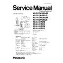
Read Panasonic KX-TCD410RUM / KX-TCD410RUS / KX-TCD412RUM / KX-TCD412RUS / KX-A141RUM / KX-A141RUS / KX-A142RUM / KX-A142RUS Service Manual online
KX-TCD410RUM
KX-TCD410RUS
KX-TCD412RUM
KX-TCD412RUS
KX-A141RUM
KX-A141RUS
KX-A142RUM
KX-A142RUS
Digital Cordless Phone
Metalic Gray Version
Silver Version
(for Russia)
Silver Version
(for Russia)
Telephone Equipment
ORDER NO. KM40306109C3
1 ABOUT LEAD FREE SOLDER (PbF: Pb free)
4
1.1. Suggested PbF Solder
4
1.2. Howto recognize that Pb Free solder is used
5
2 FOR SERVICE TECHNICIANS
7
3 CAUTION
7
4 BATTERY
8
4.1. Battery Installation
8
4.2. Battery Charge
8
4.3. Battery Life
9
4.4. Replacing the Batteries
9
5 LOCATION OF CONTROLS
10
5.1. Base Unit
10
5.2. Handset
10
6 SETTINGS
11
6.1. Connection
11
6.2. Symbols Used in This Service Manual
11
6.3. PIN Code
12
6.4. Reset
14
6.5. Key Lock
15
6.6. Recall Feature
15
6.7. Dialling Pause for PBX line/long distance service users 15
6.8. Call Restriction
6.8. Call Restriction
16
6.9. Cancelling Call Restricted Handset(s)
16
6.10. Call BAR On/Off (Call Prohibition On/Off)
16
6.11. Selecting the Display Language
17
6.12. Select Dialling Mode (Tone/Pulse)
17
6.13. Select Flash Timing
17
6.14. Automatic Route Selection
18
6.15. Summary of Programmable Functions
20
7 DISPLAY
20
7.1. Handset Display
20
7.2. Before Requesting Help (Troubleshooting)
21
8 OPERATIONS
22
8.1. Power On/Off
22
8.2. Making a Call
22
8.3. Answering a Call
22
8.4. Setting the Clock/Date
22
8.5. Phonebook
23
9 DISASSEMBLY INSTRUCTIONS
26
9.1. Base Unit
26
9.2. Handset
27
9.3. Charger Unit
28
10 ASSEMBLY INSTRUCTIONS
29
10.1. Warning When Constructing the Base Unit
29
11 TROUBLESHOOTING GUIDE
30
11.1. Check Power
31
11.2. Check Battery Charge
32
11.3. Check Link
33
11.4. Check Handset Transmission
35
11.5. Check Handset Reception
35
11.6. Check Caller ID
35
11.7. Bell Reception
36
12 CHECK PROCEDURE (BASE UNIT)
37
12.1. Preparation
37
12.2. PC Setting
37
13 CHECK PROCEDURE (HANDSET)
38
13.1. Preparation
38
13.2. PC Setting
38
14 ADJUSTMENTS (BASE UNIT AND CHARGER UNIT)
39
14.1. Adjustment (Base Unit)
39
14.2. Adjustment Standard (Base Unit)
43
14.3. Adjustment (Charger Unit)
45
14.4. Adjustment Standard (Charger Unit)
45
15 ADJUSTMENTS (HANDSET)
46
15.1. Adjustment
46
15.2. Adjustment Standard (Handset)
49
16 RF SPECIFICATION
50
16.1. Base Unit
50
16.2. Handset
50
17 HOW TO CHECK THE HANDSET SPEAKER
50
18 FREQUENCY TABLE (MHz)
51
19 BLOCK DIAGRAM (BASE UNIT)
52
20 CIRCUIT OPERATION (BASE UNIT)
53
20.1. Outline
53
20.2. Power Supply Circuit
54
20.3. Telephone Line Interface
55
20.4. Transmitter/Receiver
55
20.5. Pulse Dialing
55
20.6. FLASH PROM
55
21 BLOCK DIAGRAM (HANDSET)
56
CONTENTS
Page
Page
2
KX-TCD410RUM / KX-TCD410RUS / KX-TCD412RUM / KX-TCD412RUS / KX-A141RUM / KX-A141RUS / KX-A142RUM / KX-A142RUS
22 CIRCUIT OPERATION (HANDSET)
57
22.1. Outline
57
22.2. Power Supply Circuit/Reset Circuit
57
22.3. Charge Circuit
57
22.4. Battery Low/Power Down Detector
57
23 CIRCUIT OPERATION (CHARGER UNIT)
58
23.1. Power Supply Circuit
58
24 SIGNAL ROUTE
58
25 CPU DATA (BASE UNIT)
59
25.1. IC2 (BBIC)
59
26 CPU DATA (HANDSET)
61
26.1. IC1 (BBIC)
61
27 EEPROM LAYOUT (BASE UNIT)
63
27.1. Scope
63
27.2. Introduction
63
27.3. EEPROM Layout
63
28 EEPROM LAYOUT (HANDSET)
66
28.1. Scope
66
28.2. Introduction
66
28.3. EEPROM contents
66
29 HOW TO REPLACE FLAT PACKAGE IC
69
29.1. Preparation
69
29.2. Procedure
69
29.3. Modification Procedure of Bridge
69
30 CABINET AND ELECTRICAL PARTS LOCATION (BASE UNIT)
70
31 CABINET AND ELECTRICAL PARTS LOCATION (HANDSET) 71
32 CABINET AND ELECTRICAL PARTS LOCATION (CHARGER
32 CABINET AND ELECTRICAL PARTS LOCATION (CHARGER
UNIT)
72
33 ACCESSORIES AND PACKING MATERIALS
73
33.1. KX-TCD410RUM/RUS
73
33.2. KX-TCD412RUM/RUS
74
33.3. KX-A142RUM/RUS
75
34 TERMINAL GUIDE OF THE ICs, TRANSISTORS AND DIODES
76
34.1. Base Unit
76
34.2. Handset
76
34.3. Charger Unit
76
35 REPLACEMENT PARTS LIST
77
35.1. Base Unit
77
35.2. Handset
78
35.3. Charger Unit
79
35.4. Accessories and Packing Materials
79
35.5. Fixtures and Tools
80
36 SCHEMATIC DIAGRAM (BASE UNIT)
81
37 SCHEMATIC DIAGRAM (HANDSET)
83
38 SCHEMATIC DIAGRAM (CHARGER UNIT)
85
39 CIRCUIT BOARD (BASE UNIT)
86
39.1. Component View
86
39.2. FlowSolder Side View
87
40 CIRCUIT BOARD (HANDSET)
88
40.1. Component View
88
40.2. FlowSolder Side View
89
41 CIRCUIT BOARD (CHARGER UNIT)
90
41.1. Component View
90
41.2. FlowSolder Side View
90
3
KX-TCD410RUM / KX-TCD410RUS / KX-TCD412RUM / KX-TCD412RUS / KX-A141RUM / KX-A141RUS / KX-A142RUM / KX-A142RUS
1 ABOUT LEAD FREE SOLDER (PbF: Pb free)
Note:
In the information below, Pb, the symbol for lead in the periodic table of elements, will refer to standard solder or solder that
contains lead.
We will use PbF solder when discussing the lead free solder used in our manufacturing process which is made from Tin (Sn),
Silver (Ag), and Copper (Cu).
This model, and others like it, manufactured using lead free solder will have PbF stamped on the PCB. For service and repair
work we suggest using the same type of solder although, with some precautions, standard Pb solder can also be used.
Caution
·
PbF solder has a melting point that is 50°F ~70°F (30°C ~ 40°C)higher than Pb solder. Please use a soldering iron with
temperature control and adjust it to 700°F ± 20°F (370°C ± 10°C). In case of using high temperature soldering iron, please
be careful not to heat too long.
temperature control and adjust it to 700°F ± 20°F (370°C ± 10°C). In case of using high temperature soldering iron, please
be careful not to heat too long.
·
PbF solder will tend to splash if it is heated much higher than its melting point, approximately 1100°F (600°C).
·
If you must use Pb solder on a PCB manufactured using PbF solder, remove as much of the original PbF solder as possible
and be sure that any remaining is melted prior to applying the Pb solder.
and be sure that any remaining is melted prior to applying the Pb solder.
·
When applying PbF solder to double layered boards, please check the component side for excess which may flow onto the
opposite side (See the figure below).
opposite side (See the figure below).
1.1. Suggested PbF Solder
There are several types of PbF solder available commercially. While this product is manufactured using Tin, Silver, and Copper
(Sn+Ag+Cu), you can also use Tin and Copper (Sn+Cu) or Tin, Zinc, and Bismuth (Sn+Zn+Bi). Please check the manufac
turers specific instructions for the melting points of their products and any precautions for using their product with other
materials.
The following lead free (PbF)solder wire sizes are recommended for service of this product: 0.3mm, 0.6mm and 1.0mm.
4
KX-TCD410RUM / KX-TCD410RUS / KX-TCD412RUM / KX-TCD412RUS / KX-A141RUM / KX-A141RUS / KX-A142RUM / KX-A142RUS


