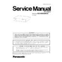
Read Panasonic KX-NS8290CE Service Manual online
ORDER NO. KMS1211915CE
PRI Adaptor
Model No.
KX-NS8290CE
(for Europe)
2
KX-NS8290
TABLE OF CONTENTS
PAGE
PAGE
1 Safety Precautions -----------------------------------------------3
1.1. For Service Technicians ---------------------------------3
2 Warning --------------------------------------------------------------4
2.1. Caution--------------------------------------------------------4
2.2. About Lead Free Solder (PbF: Pb free) --------------4
2.2. About Lead Free Solder (PbF: Pb free) --------------4
2.2.1. Suggested PbF Solder -------------------------------5
2.3. Discarding of P. C. Board --------------------------------5
3 Specifications ------------------------------------------------------6
3.1. General Description ---------------------------------------6
3.2. System Capacity -------------------------------------------6
3.2. System Capacity -------------------------------------------6
4 Technical Descriptions------------------------------------------7
4.1. System Block Diagram------------------------------------7
4.2. Hardware Specification -----------------------------------8
4.2. Hardware Specification -----------------------------------8
4.2.1. Hardware Detail Specifications --------------------8
4.2.2. DSP Block Detail Specifications -------------------9
4.2.3. Line Interface Block Detail Specifications ----- 10
4.2.2. DSP Block Detail Specifications -------------------9
4.2.3. Line Interface Block Detail Specifications ----- 10
4.3. CPU GPIO Port List ------------------------------------- 11
4.4. CPU BUS Interface Block Diagram------------------ 12
4.5. Interrupt FUnction---------------------------------------- 12
4.6. Reset Function-------------------------------------------- 13
4.7. LED Interface---------------------------------------------- 13
4.8. 4.9LAN Port Interface ----------------------------------- 14
4.9. TDM-BUS Interface-------------------------------------- 14
4.9.1. TDM-BUS Signal Connection -------------------- 14
4.9.2. TDM-BUS Timing Specifications----------------- 15
4.9.2. TDM-BUS Timing Specifications----------------- 15
4.10. Power Plane ----------------------------------------------- 16
4.10.1. Power Plane Block Diagram---------------------- 16
4.10.2. Power Supply and Reset Sequence------------ 16
4.10.3. Power Supply Interruption Backup Circuit ---- 17
4.10.4. Power Supply Interruption Detection
4.10.2. Power Supply and Reset Sequence------------ 16
4.10.3. Power Supply Interruption Backup Circuit ---- 17
4.10.4. Power Supply Interruption Detection
Circuit--------------------------------------------------- 17
4.10.5. PoE (IEEE 802.3af Class2) ----------------------- 18
4.10.6. AC-Adaptor ------------------------------------------- 18
4.10.6. AC-Adaptor ------------------------------------------- 18
5 Location of Controls and Components------------------ 19
5.1. Name and Locations ------------------------------------ 19
5.2. LED Indications ------------------------------------------- 20
5.2. LED Indications ------------------------------------------- 20
6 Installation Instructions--------------------------------------- 21
6.1. System Connection Diagram-------------------------- 21
7 Test Mode---------------------------------------------------------- 22
7.1. Utility--------------------------------------------------------- 22
7.1.1. Utility—Diagnosis------------------------------------ 22
7.1.2. Utility—File -------------------------------------------- 22
7.1.3. Utility—Log-------------------------------------------- 24
7.1.4. Utility—Monitor/Trace ------------------------------ 25
7.1.5. Utility—Report---------------------------------------- 26
7.1.2. Utility—File -------------------------------------------- 22
7.1.3. Utility—Log-------------------------------------------- 24
7.1.4. Utility—Monitor/Trace ------------------------------ 25
7.1.5. Utility—Report---------------------------------------- 26
8 Troubleshooting Guide---------------------------------------- 27
8.1. Power Circuit Check Flowchart----------------------- 28
8.2. Clock / Reset / NOR Flash Check Flowchart ----- 29
8.3. NAND Flash Check Flowchart ------------------------ 30
8.4. Application Program Trouble ------------------------- 30
8.5. Communication Trouble -------------------------------- 31
8.6. Speech Noise Trouble ---------------------------------- 32
9 Disassembly and Assembly Instructions--------------- 33
9.1. Remove Main Board------------------------------------- 33
9.2. Disassembly for Main Board -------------------------- 34
9.2. Disassembly for Main Board -------------------------- 34
10 Miscellaneous --------------------------------------------------- 35
10.1. How To Replace a Flat Package IC----------------- 35
10.1.1. Preparation ------------------------------------------- 35
10.1.2. Removal Procedure -------------------------------- 35
10.1.3. Procedure--------------------------------------------- 35
10.1.4. Removing Solder From Between Pins--------- 35
10.1.2. Removal Procedure -------------------------------- 35
10.1.3. Procedure--------------------------------------------- 35
10.1.4. Removing Solder From Between Pins--------- 35
10.2. How to Replace the LLP (Leadless Leadframe
Package) IC and IC ground plate-------------------- 36
10.2.1. Preparation ------------------------------------------- 36
10.2.2. Caution ------------------------------------------------ 36
10.2.3. How to Remove the IC ---------------------------- 36
10.2.4. How to Install the IC-------------------------------- 36
10.2.5. How to Remove a Solder Bridge (Doesn't
10.2.2. Caution ------------------------------------------------ 36
10.2.3. How to Remove the IC ---------------------------- 36
10.2.4. How to Install the IC-------------------------------- 36
10.2.5. How to Remove a Solder Bridge (Doesn't
apply to IC ground plate.) ------------------------- 37
10.3. Terminal Guide of the ICs, Transistors and
Diodes ------------------------------------------------------ 38
10.4. Memo ------------------------------------------------------- 39
11 Schematic Diagram -------------------------------------------- 40
11.1. No. 1 -------------------------------------------------------- 40
11.2. No. 2 -------------------------------------------------------- 42
11.3. No. 3 -------------------------------------------------------- 44
11.4. No. 4 -------------------------------------------------------- 46
11.5. Waveform-------------------------------------------------- 48
11.2. No. 2 -------------------------------------------------------- 42
11.3. No. 3 -------------------------------------------------------- 44
11.4. No. 4 -------------------------------------------------------- 46
11.5. Waveform-------------------------------------------------- 48
11.5.1. Test Point Waveform ------------------------------- 48
11.5.2. LAN Port Waveform -------------------------------- 50
11.5.3. DC-DC Converter (3.3V) Waveform------------ 51
11.5.4. DC-DC Converter (1.1V) Waveform------------ 51
11.5.5. PoE Circuit Waveform ----------------------------- 52
11.5.6. Power & Reset Signal Waveform --------------- 52
11.5.7. NOR-Flash Memory Access Waveform ------- 52
11.5.8. NAND-Flash Memory Access Waveform ----- 53
11.5.9. TDM-BUS Access Waveform -------------------- 54
12 Printed Circuit Board------------------------------------------ 55
12.1. Component View----------------------------------------- 55
12.2. Bottom View----------------------------------------------- 56
12.2. Bottom View----------------------------------------------- 56
13 Appendix Information of Schematic Diagram -------- 57
14 Exploded View and Replacement Parts List----------- 58
14 Exploded View and Replacement Parts List----------- 58
14.1. Cabinet and Electrical Parts -------------------------- 58
14.2. Accessories and Packing Materials----------------- 59
14.3. Replacement Parts List -------------------------------- 60
14.2. Accessories and Packing Materials----------------- 59
14.3. Replacement Parts List -------------------------------- 60
14.3.1. Cabinet and Electrical Parts---------------------- 60
14.3.2. Accessories and Packing Materials ------------ 60
14.3.3. Main Board Parts ----------------------------------- 60
14.3.2. Accessories and Packing Materials ------------ 60
14.3.3. Main Board Parts ----------------------------------- 60
3
KX-NS8290
1 Safety Precautions
1. Before servicing, unplug the AC power cord to prevent an electric shock.
2. When replacing parts, use only the manufacturer's recommended components.
3. Check the condition of the power cord. Replace if wear or damage is evident.
4. After servicing, be sure to restore the lead dress, insulation barriers, insulation papers, shields, etc.
5. Before returning the serviced equipment to the customer, be sure to perform the following insulation resistance test to prevent
the customer from being exposed to shock hazards.
1.1.
For Service Technicians
• Repair service shall be provided in accordance with repair technology information such as service manual so as to prevent fires,
injury or electric shock, which can be caused by improper repair work.
1. When repair services are provided, neither the products nor their parts or members shall be remodeled.
2. If a lead wire assembly is supplied as a repair part, the lead wire assembly shall be replaced.
3. FASTON terminals shall be plugged straight in and unplugged straight out.
2. If a lead wire assembly is supplied as a repair part, the lead wire assembly shall be replaced.
3. FASTON terminals shall be plugged straight in and unplugged straight out.
• ICs and LSIs are vulnerable to static electricity.
When repairing, the following precautions will help prevent recurring malfunctions.
1. Cover plastic parts boxes with aluminum foil.
2. Ground the soldering irons.
3. Use a conductive mat on worktable.
4. Do not grasp IC or LSI pins with bare fingers.
2. Ground the soldering irons.
3. Use a conductive mat on worktable.
4. Do not grasp IC or LSI pins with bare fingers.
4
KX-NS8290
2 Warning
2.1.
Caution
The power socket wall outlet should be located near this equipment and be easily accessible.
2.1. VORSICHT
2.2.
About Lead Free Solder (PbF: Pb free)
Note:
In the information below, Pb, the symbol for lead in the periodic table of elements, will refer to standard solder or solder that con-
tains lead.
We will use PbF when discussing the lead free solder used in our manufacturing process which is made from Tin, (Sn), Silver,
(Ag), and Copper, (Cu).
This model, and others like it, manufactured using lead free solder will have PbF stamped on the PCB. For service and repair
work we suggest using the same type of solder.
Caution
• PbF solder has a melting point that is 50
° ~ 70° F, (30° ~ 40°C) higher than Pb solder. Please use a soldering iron with tempera-
ture control and adjust it to 700
° ± 20° F, (370° ± 10°C).
Exercise care while using higher temperature soldering irons.:
Do not heat the PCB for too long time in order to prevent solder splash or damage to the PCB.
Do not heat the PCB for too long time in order to prevent solder splash or damage to the PCB.
• PbF solder will tend to splash if it is heated much higher than its melting point, approximately 1100
°F, (600°C).
• When applying PbF solder to double layered boards, please check the component side for excess which may flow onto the
opposite side (See figure, below).


